ZHCSGS4A
August 2017 – February 2020
ADS114S06B
,
ADS114S08B
PRODUCTION DATA.
1
特性
2
应用
3
说明
Device Images
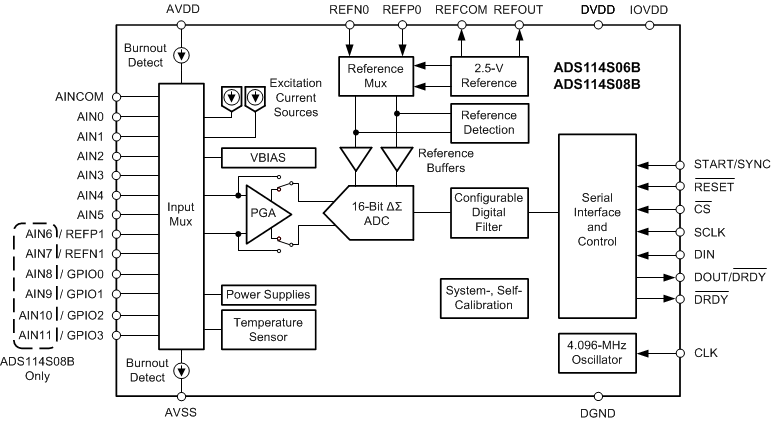
功能方框图
4
修订历史记录
5
Device Comparison Table
6
Pin Configuration and Functions
Pin Functions
7
Specifications
7.1
Absolute Maximum Ratings
7.2
ESD Ratings
7.3
Recommended Operating Conditions
7.4
Thermal Information
7.5
Electrical Characteristics
7.6
Timing Requirements
7.7
Switching Characteristics
7.8
Typical Characteristics
8
Parameter Measurement Information
8.1
Noise Performance
9
Detailed Description
9.1
Overview
9.2
Functional Block Diagram
9.3
Feature Description
9.3.1
Multiplexer
9.3.2
Low-Noise Programmable Gain Amplifier
9.3.2.1
PGA Input-Voltage Requirements
9.3.2.2
Bypassing the PGA
9.3.3
Voltage Reference
9.3.3.1
Internal Reference
9.3.3.2
External Reference
9.3.3.3
Reference Buffers
9.3.4
Clock Source
9.3.5
Delta-Sigma Modulator
9.3.6
Digital Filter
9.3.6.1
Digital Filter Frequency Response
9.3.6.2
Data Conversion Time
9.3.6.3
Note on Conversion Time
9.3.6.4
50-Hz and 60-Hz Line Cycle Rejection
9.3.7
Excitation Current Sources (IDACs)
9.3.8
Bias Voltage Generation
9.3.9
System Monitor
9.3.9.1
Internal Temperature Sensor
9.3.9.2
Power Supply Monitors
9.3.9.3
Burn-Out Current Sources
9.3.10
Status Register
9.3.10.1
POR Flag
9.3.10.2
RDY Flag
9.3.10.3
External Reference Monitor
9.3.11
General-Purpose Inputs and Outputs (GPIOs)
9.3.12
Calibration
9.3.12.1
Offset Calibration
9.3.12.2
Gain Calibration
9.4
Device Functional Modes
9.4.1
Reset
9.4.1.1
Power-On Reset
9.4.1.2
RESET Pin
9.4.1.3
Reset by Command
9.4.2
Power-Down Mode
9.4.3
Standby Mode
9.4.4
Conversion Modes
9.4.4.1
Continuous Conversion Mode
9.4.4.2
Single-Shot Conversion Mode
9.5
Programming
9.5.1
Serial Interface
9.5.1.1
Chip Select (CS)
9.5.1.2
Serial Clock (SCLK)
9.5.1.3
Serial Data Input (DIN)
9.5.1.4
Serial Data Output and Data Ready (DOUT/DRDY)
9.5.1.5
Data Ready (DRDY)
9.5.1.6
Timeout
9.5.2
Data Format
9.5.3
Commands
9.5.3.1
NOP
9.5.3.2
WAKEUP
9.5.3.3
POWERDOWN
9.5.3.4
RESET
9.5.3.5
START
9.5.3.6
STOP
9.5.3.7
SYOCAL
9.5.3.8
SYGCAL
9.5.3.9
SFOCAL
9.5.3.10
RDATA
9.5.3.11
RREG
9.5.3.12
WREG
9.5.4
Interfacing with Multiple Devices
9.6
Register Map
9.6.1
Configuration Registers
9.6.2
Register Descriptions
9.6.2.1
Device ID Register (address = 00h) [reset = xxh]
Table 16.
Device ID (ID) Register Field Descriptions
9.6.2.2
Device Status Register (address = 01h) [reset = 80h]
Table 17.
Device Status (STATUS) Register Field Descriptions
9.6.2.3
Input Multiplexer Register (address = 02h) [reset = 01h]
Table 18.
Input Multiplexer (INPMUX) Register Field Descriptions
9.6.2.4
Gain Setting Register (address = 03h) [reset = 00h]
Table 19.
Gain Setting (PGA) Register Field Descriptions
9.6.2.5
Data Rate Register (address = 04h) [reset = 14h]
Table 20.
Data Rate (DATARATE) Register Field Descriptions
9.6.2.6
Reference Control Register (address = 05h) [reset = 10h]
Table 21.
Reference Control (REF) Register Field Descriptions
9.6.2.7
Excitation Current Register 1 (address = 06h) [reset = 00h]
Table 22.
Excitation Current Register 1 (IDACMAG) Register Field Descriptions
9.6.2.8
Excitation Current Register 2 (address = 07h) [reset = FFh]
Table 23.
Excitation Current Register 2 (IDACMUX) Register Field Descriptions
9.6.2.9
Sensor Biasing Register (address = 08h) [reset = 00h]
Table 24.
Sensor Biasing (VBIAS) Register Field Descriptions
9.6.2.10
System Control Register (address = 09h) [reset = 10h]
Table 25.
System Control (SYS) Register Field Descriptions
9.6.2.11
Reserved Register (address = 0Ah) [reset = 00h]
Table 26.
Reserved Register Field Descriptions
9.6.2.12
Offset Calibration Register 1 (address = 0Bh) [reset = 00h]
Table 27.
Offset Calibration Register 1 (OFCAL0) Register Field Descriptions
9.6.2.13
Offset Calibration Register 2 (address = 0Ch) [reset = 00h]
Table 28.
Offset Calibration Register 2 (OFCAL1) Register Field Descriptions
9.6.2.14
Reserved Register (address = 0Dh) [reset = 00h]
Table 29.
Reserved Register Field Descriptions
9.6.2.15
Gain Calibration Register 1 (address = 0Eh) [reset = 00h]
Table 30.
Gain Calibration Register 1 (FSCAL0) Field Descriptions
9.6.2.16
Gain Calibration Register 2 (address = 0Fh) [reset = 40h]
Table 31.
Gain Calibration Register 2 (FSCAL1) Field Descriptions
9.6.2.17
GPIO Data Register (address = 10h) [reset = 00h]
Table 32.
GPIO Data (GPIODAT) Register Field Descriptions
9.6.2.18
GPIO Configuration Register (address = 11h) [reset = 00h]
Table 33.
GPIO Configuration (GPIOCON) Register Field Descriptions
10
Application and Implementation
10.1
Application Information
10.1.1
Serial Interface Connections
10.1.2
Analog Input Filtering
10.1.3
External Reference and Ratiometric Measurements
10.1.4
Establishing a Proper Input Voltage
10.1.5
Unused Inputs and Outputs
10.1.6
Pseudo Code Example
10.2
Typical Application
10.2.1
Design Requirements
10.2.2
Detailed Design Procedure
10.2.2.1
Register Settings
10.2.3
Application Curves
10.3
What To Do and What Not To Do
11
Power Supply Recommendations
11.1
Power Supplies
11.2
Power-Supply Sequencing
11.3
Power-On Reset
11.4
Power-Supply Decoupling
12
Layout
12.1
Layout Guidelines
12.2
Layout Example
13
器件和文档支持
13.1
器件支持
13.1.1
开发支持
13.2
文档支持
13.2.1
相关文档
13.3
相关链接
13.4
接收文档更新通知
13.5
社区资源
13.6
商标
13.7
静电放电警告
13.8
Glossary
14
机械、封装和可订购信息
封装选项
请参考 PDF 数据表获取器件具体的封装图。
机械数据 (封装 | 引脚)
RHB|32
PBS|32
散热焊盘机械数据 (封装 | 引脚)
PBS|32
QFND381
订购信息
zhcsgs4a_oa
zhcsgs4a_pm
Device Images
功能方框图
千亿体育app官网登录(中国)官方网站IOS/安卓通用版/手机APP
|
米乐app下载官网(中国)|ios|Android/通用版APP最新版
|
米乐|米乐·M6(中国大陆)官方网站
|
千亿体育登陆地址
|
华体会体育(中国)HTH·官方网站
|
千赢qy国际_全站最新版千赢qy国际V6.2.14安卓/IOS下载
|
18新利网v1.2.5|中国官方网站
|
bob电竞真人(中国官网)安卓/ios苹果/电脑版【1.97.95版下载】
|
千亿体育app官方下载(中国)官方网站IOS/安卓/手机APP下载安装
|