ZHCSQZ9A March   2022  – October 2022 ADS117L11

PRODUCTION DATA  

  1. 特性
  2. 应用
  3. 说明
  4. Revision History
  5. Pin Configuration and Functions
  6. Specifications
    1. 6.1  Absolute Maximum Ratings
    2. 6.2  ESD Ratings
    3. 6.3  Recommended Operating Conditions
    4. 6.4  Thermal Information
    5. 6.5  Electrical Characteristics
    6. 6.6  Timing Requirements (1.65 V ≤ IOVDD ≤ 2 V)
    7. 6.7  Switching Characteristics (1.65 V ≤ IOVDD ≤ 2 V)
    8. 6.8  Timing Requirements (2 V < IOVDD ≤ 5.5 V)
    9. 6.9  Switching Characteristics (2 V < IOVDD ≤ 5.5 V)
    10. 6.10 Timing Diagrams
    11. 6.11 Typical Characteristics
  7. Parameter Measurement Information
    1. 7.1  Offset Error Measurement
    2. 7.2  Offset Drift Measurement
    3. 7.3  Gain Error Measurement
    4. 7.4  Gain Drift Measurement
    5. 7.5  NMRR Measurement
    6. 7.6  CMRR Measurement
    7. 7.7  PSRR Measurement
    8. 7.8  INL Error Measurement
    9. 7.9  THD Measurement
    10. 7.10 SFDR Measurement
    11. 7.11 Noise Performance
  8. Detailed Description
    1. 8.1 Overview
    2. 8.2 Functional Block Diagram
    3. 8.3 Feature Description
      1. 8.3.1 Analog Input (AINP, AINN)
        1. 8.3.1.1 Input Range
      2. 8.3.2 Reference Voltage (REFP, REFN)
        1. 8.3.2.1 Reference Voltage Range
      3. 8.3.3 Clock Operation
        1. 8.3.3.1 Internal Oscillator
        2. 8.3.3.2 External Clock
      4. 8.3.4 Modulator
      5. 8.3.5 Digital Filter
        1. 8.3.5.1 Wideband Filter
        2. 8.3.5.2 Low-Latency Filter (Sinc)
          1. 8.3.5.2.1 Sinc4 Filter
          2. 8.3.5.2.2 Sinc4 + Sinc1 Filter
          3. 8.3.5.2.3 Sinc3 Filter
          4. 8.3.5.2.4 Sinc3 + Sinc1 Filter
      6. 8.3.6 Power Supplies
        1. 8.3.6.1 AVDD1 and AVSS
        2. 8.3.6.2 AVDD2
        3. 8.3.6.3 IOVDD
        4. 8.3.6.4 Power-On Reset (POR)
        5. 8.3.6.5 CAPA and CAPD
      7. 8.3.7 VCM Output Voltage
    4. 8.4 Device Functional Modes
      1. 8.4.1 Power-Scalable Speed Modes
      2. 8.4.2 Idle Mode
      3. 8.4.3 Standby Mode
      4. 8.4.4 Power-Down Mode
      5. 8.4.5 Reset
        1. 8.4.5.1 RESET Pin
        2. 8.4.5.2 Reset by SPI Register Write
        3. 8.4.5.3 Reset by SPI Input Pattern
      6. 8.4.6 Synchronization
        1. 8.4.6.1 Synchronized Control Mode
        2. 8.4.6.2 Start/Stop Control Mode
        3. 8.4.6.3 One-Shot Control Mode
      7. 8.4.7 Conversion-Start Delay Time
      8. 8.4.8 Calibration
        1. 8.4.8.1 OFFSET2, OFFSET1, OFFSET0 Calibration Registers (Addresses 9h, Ah, Bh)
        2. 8.4.8.2 GAIN2, GAIN1, GAIN0 Calibration Registers (Addresses 0Ch, 0Dh, 0Eh)
        3. 8.4.8.3 Calibration Procedure
    5. 8.5 Programming
      1. 8.5.1 Serial Interface (SPI)
        1. 8.5.1.1 Chip Select (CS)
        2. 8.5.1.2 Serial Clock (SCLK)
        3. 8.5.1.3 Serial Data Input (SDI)
        4. 8.5.1.4 Serial Data Output/Data Ready (SDO/DRDY)
      2. 8.5.2 SPI Frame
      3. 8.5.3 SPI CRC
      4. 8.5.4 Register Map CRC
      5. 8.5.5 Full-Duplex Operation
      6. 8.5.6 Device Commands
        1. 8.5.6.1 No-Operation
        2. 8.5.6.2 Read Register Command
        3. 8.5.6.3 Write Register Command
      7. 8.5.7 Read Conversion Data
        1. 8.5.7.1 Conversion Data
        2. 8.5.7.2 Data Ready
          1. 8.5.7.2.1 DRDY
          2. 8.5.7.2.2 SDO/DRDY
          3. 8.5.7.2.3 DRDY Bit
          4. 8.5.7.2.4 Clock Counting
        3. 8.5.7.3 STATUS Header
      8. 8.5.8 Daisy-Chain Operation
      9. 8.5.9 3-Wire SPI Mode
        1. 8.5.9.1 3-Wire SPI Mode Frame Reset
    6. 8.6 Registers
      1. 8.6.1  DEV_ID Register (Address = 0h) [reset = 01h]
      2. 8.6.2  REV_ID Register (Address = 1h) [reset = xxh]
      3. 8.6.3  STATUS Register (Address = 2h) [reset = x1100xxxb]
      4. 8.6.4  CONTROL Register (Address = 3h) [reset = 00h]
      5. 8.6.5  MUX Register (Address = 4h) [reset = 00h]
      6. 8.6.6  CONFIG1 Register (Address = 5h) [reset = 00h]
      7. 8.6.7  CONFIG2 Register (Address = 6h) [reset = 00h]
      8. 8.6.8  CONFIG3 Register (Address = 7h) [reset = 00h]
      9. 8.6.9  CONFIG4 Register (Address = 8h) [reset = 08h]
      10. 8.6.10 OFFSET2, OFFSET1, OFFSET0 Registers (Addresses = 9h, Ah, Bh) [reset = 00h, 00h, 00h]
      11. 8.6.11 GAIN2, GAIN1, GAIN0 Registers (Addresses = Ch, Dh, Eh) [reset = 40h, 00h, 00h]
      12. 8.6.12 CRC Register (Address = Fh) [reset = 00h]
  9. Application and Implementation
    1. 9.1 Application Information
      1. 9.1.1 Input Driver
      2. 9.1.2 Antialias Filter
      3. 9.1.3 Reference Voltage
      4. 9.1.4 Simultaneous-Sampling Systems
    2. 9.2 Typical Application
      1. 9.2.1 Design Requirements
      2. 9.2.2 Detailed Design Procedure
      3. 9.2.3 Application Curves
    3. 9.3 Power Supply Recommendations
    4. 9.4 Layout
      1. 9.4.1 Layout Guidelines
      2. 9.4.2 Layout Example
  10. 10Device and Documentation Support
    1. 10.1 Documentation Support
      1. 10.1.1 Related Documentation
    2. 10.2 接收文档更新通知
    3. 10.3 支持资源
    4. 10.4 Trademarks
    5. 10.5 Electrostatic Discharge Caution
    6. 10.6 术语表
  11. 11Mechanical, Packaging, and Orderable Information
    1. 11.1 Mechanical Data

封装选项

请参考 PDF 数据表获取器件具体的封装图。

机械数据 (封装 | 引脚)
  • RUK|20
散热焊盘机械数据 (封装 | 引脚)
订购信息
Sinc3 + Sinc1 Filter

The sinc3 + sinc1 filter mode is the cascade of the sinc3 and the sinc1 filter. The OSR of the sinc3 stage is fixed (32000) and the OSR of the sinc1 stage is programmable to 3 and 5. Table 8-7 summarizes the characteristics of the sinc3 + sinc1 filter.

Table 8-7 Sinc3 + Sinc1 Filter Characteristics
SINC3 OSRSINC1 OSRDATA RATE (SPS)–3-dB FREQUENCY (HZ)LATENCY (ms)REJECTION OF FIRST NULL (dB)
2% CLOCK TOLERANCE6% CLOCK TOLERANCE
HIGH-SPEED MODE (fCLK = 25.6 MHz)
320003133.35412.53726
320005803417.53726
LOW-SPEED MODE (fCLK = 3.2 MHz)
32000316.76.7100.13426
320005104.2140.013426

Figure 8-19 shows the frequency response of the sinc3 + sinc1 filter. The frequency response exhibits the characteristic sinc filter response lobes and nulls. The nulls occur at fDATA and at multiples thereof. Figure 8-20 shows the detailed response in the region of 0.9 to 1.1 · fIN / fDATA.
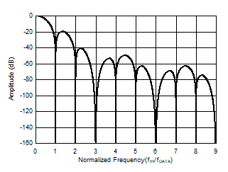
GUID-AF122C95-3B18-410C-9430-B5C5DE5870B4-low.gifFigure 8-19 Sinc3 + Sinc1 Frequency Response
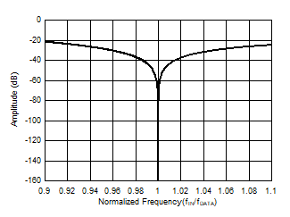
GUID-521FE6B3-DCEA-4ACB-975C-025ED1A16D11-low.gifFigure 8-20 Detail Sinc3 + Sinc1 Frequency Response