ZHCSHW6B October   2017  – October 2018 ADS122C04

PRODUCTION DATA.  

  1. 特性
  2. 应用
  3. 说明
    1.     Device Images
      1.      K 型热电偶测量
  4. 修订历史记录
  5. Pin Configuration and Functions
    1.     Pin Functions
  6. Specifications
    1. 6.1 Absolute Maximum Ratings
    2. 6.2 ESD Ratings
    3. 6.3 Recommended Operating Conditions
    4. 6.4 Thermal Information
    5. 6.5 Electrical Characteristics
    6. 6.6 I2C Timing Requirements
    7. 6.7 I2C Switching Characteristics
    8. 6.8 Typical Characteristics
  7. Parameter Measurement Information
    1. 7.1 Noise Performance
  8. Detailed Description
    1. 8.1 Overview
    2. 8.2 Functional Block Diagram
    3. 8.3 Feature Description
      1. 8.3.1  Multiplexer
      2. 8.3.2  Low-Noise Programmable Gain Stage
        1. 8.3.2.1 PGA Input Voltage Requirements
        2. 8.3.2.2 Bypassing the PGA
      3. 8.3.3  Voltage Reference
      4. 8.3.4  Modulator and Internal Oscillator
      5. 8.3.5  Digital Filter
      6. 8.3.6  Conversion Times
      7. 8.3.7  Excitation Current Sources
      8. 8.3.8  Sensor Detection
      9. 8.3.9  System Monitor
      10. 8.3.10 Temperature Sensor
        1. 8.3.10.1 Converting From Temperature to Digital Codes
          1. 8.3.10.1.1 For Positive Temperatures (For Example, 50°C):
          2. 8.3.10.1.2 For Negative Temperatures (For Example, –25°C):
        2. 8.3.10.2 Converting From Digital Codes to Temperature
      11. 8.3.11 Offset Calibration
      12. 8.3.12 Conversion Data Counter
      13. 8.3.13 Data Integrity Features
    4. 8.4 Device Functional Modes
      1. 8.4.1 Power-Up and Reset
        1. 8.4.1.1 Power-On Reset
        2. 8.4.1.2 RESET Pin
        3. 8.4.1.3 Reset by Command
      2. 8.4.2 Conversion Modes
        1. 8.4.2.1 Single-Shot Conversion Mode
        2. 8.4.2.2 Continuous Conversion Mode
      3. 8.4.3 Operating Modes
        1. 8.4.3.1 Normal Mode
        2. 8.4.3.2 Turbo Mode
        3. 8.4.3.3 Power-Down Mode
    5. 8.5 Programming
      1. 8.5.1 I2C Interface
        1. 8.5.1.1 I2C Address
        2. 8.5.1.2 Serial Clock (SCL) and Serial Data (SDA)
        3. 8.5.1.3 Data Ready (DRDY)
        4. 8.5.1.4 Interface Speed
        5. 8.5.1.5 Data Transfer Protocol
        6. 8.5.1.6 I2C General Call (Software Reset)
        7. 8.5.1.7 Timeout
      2. 8.5.2 Data Format
      3. 8.5.3 Commands
        1. 8.5.3.1 Command Latching
        2. 8.5.3.2 RESET (0000 011x)
        3. 8.5.3.3 START/SYNC (0000 100x)
        4. 8.5.3.4 POWERDOWN (0000 001x)
        5. 8.5.3.5 RDATA (0001 xxxx)
        6. 8.5.3.6 RREG (0010 rrxx)
        7. 8.5.3.7 WREG (0100 rrxx dddd dddd)
      4. 8.5.4 Reading Data and Monitoring for New Conversion Results
      5. 8.5.5 Data Integrity
    6. 8.6 Register Map
      1. 8.6.1 Configuration Registers
      2. 8.6.2 Register Descriptions
        1. 8.6.2.1 Configuration Register 0 (address = 00h) [reset = 00h]
          1. Table 19. Configuration Register 0 Field Descriptions
        2. 8.6.2.2 Configuration Register 1 (address = 01h) [reset = 00h]
          1. Table 20. Configuration Register 1 Field Descriptions
        3. 8.6.2.3 Configuration Register 2 (address = 02h) [reset = 00h]
          1. Table 22. Configuration Register 2 Field Descriptions
        4. 8.6.2.4 Configuration Register 3 (address = 03h) [reset = 00h]
          1. Table 23. Configuration Register 3 Field Descriptions
  9. Application and Implementation
    1. 9.1 Application Information
      1. 9.1.1 Interface Connections
      2. 9.1.2 Connecting Multiple Devices on the Same I2C Bus
      3. 9.1.3 Unused Inputs and Outputs
      4. 9.1.4 Analog Input Filtering
      5. 9.1.5 External Reference and Ratiometric Measurements
      6. 9.1.6 Establishing Proper Limits on the Absolute Input Voltage
      7. 9.1.7 Pseudo Code Example
    2. 9.2 Typical Applications
      1. 9.2.1 K-Type Thermocouple Measurement (–200°C to +1250°C)
        1. 9.2.1.1 Design Requirements
        2. 9.2.1.2 Detailed Design Procedure
        3. 9.2.1.3 Application Curves
      2. 9.2.2 3-Wire RTD Measurement (–200°C to +850°C)
        1. 9.2.2.1 Design Requirements
        2. 9.2.2.2 Detailed Design Procedure
          1. 9.2.2.2.1 Design Variations for 2-Wire and 4-Wire RTD Measurements
        3. 9.2.2.3 Application Curves
      3. 9.2.3 Resistive Bridge Measurement
        1. 9.2.3.1 Design Requirements
        2. 9.2.3.2 Detailed Design Procedure
  10. 10Power Supply Recommendations
    1. 10.1 Power-Supply Sequencing
    2. 10.2 Power-Supply Decoupling
  11. 11Layout
    1. 11.1 Layout Guidelines
    2. 11.2 Layout Example
  12. 12器件和文档支持
    1. 12.1 器件支持
      1. 12.1.1 第三方米6体育平台手机版_好二三四免责声明
    2. 12.2 文档支持
      1. 12.2.1 相关文档
    3. 12.3 接收文档更新通知
    4. 12.4 社区资源
    5. 12.5 商标
    6. 12.6 静电放电警告
    7. 12.7 术语表
  13. 13机械、封装和可订购信息

封装选项

机械数据 (封装 | 引脚)
散热焊盘机械数据 (封装 | 引脚)
订购信息

Connecting Multiple Devices on the Same I2C Bus

Up to 16 ADS122C04 devices can be connected to a single I2C bus by using different address pin configurations for each device. Use the address pins, A0 and A1, to set the ADS122C04 to one of 16 different I2C addresses. Figure 69 shows an example with three ADS122C04 devices on the same I2C bus. One set of pullup resistors is required per bus line. If needed, decrease the pullup resistor values to compensate for the additional bus capacitance presented by multiple devices and increased line length.
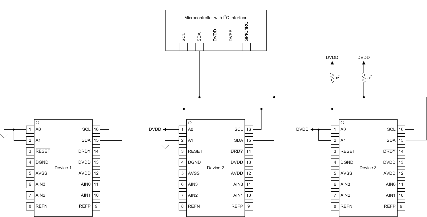
ADS122C04 ai_multi_device_connection_bas751.gifFigure 69. Connecting Multiple ADS122C04 Devices on the Same I2C Bus