ZHCSIU3 September   2018 ADS1235

PRODUCTION DATA.  

  1. 特性
  2. 应用
  3. 说明
    1.     Device Images
      1.      框图
      2.      ADC 转换噪声
  4. 修订历史记录
  5. Pin Configuration and Functions
    1.     Pin Functions
  6. Specifications
    1. 6.1 Absolute Maximum Ratings
    2. 6.2 ESD Ratings
    3. 6.3 Recommended Operating Conditions
    4. 6.4 Thermal Information
    5. 6.5 Electrical Characteristics
    6. 6.6 Timing Requirements
    7. 6.7 Switching Characteristics
    8. 6.8 Typical Characteristics
  7. Parameter Measurement Information
    1. 7.1 Noise Performance
  8. Detailed Description
    1. 8.1 Overview
    2. 8.2 Functional Block Diagram
    3. 8.3 Feature Description
      1. 8.3.1 Analog Inputs
        1. 8.3.1.1 ESD Diodes
        2. 8.3.1.2 Input Multiplexer
        3. 8.3.1.3 Temperature Sensor
        4. 8.3.1.4 Inputs Open
        5. 8.3.1.5 Internal VCOM Connection
        6. 8.3.1.6 Alternate Functions
      2. 8.3.2 PGA
        1. 8.3.2.1 Input Voltage Range
        2. 8.3.2.2 PGA Bypass Mode
      3. 8.3.3 PGA Voltage Monitor
      4. 8.3.4 Reference Voltage
        1. 8.3.4.1 External Reference
        2. 8.3.4.2 AVDD – AVSS Reference (Default)
        3. 8.3.4.3 Reference Monitor
      5. 8.3.5 General-Purpose Input/Outputs (GPIOs)
      6. 8.3.6 Modulator
      7. 8.3.7 Digital Filter
        1. 8.3.7.1 Sinc Filter
          1. 8.3.7.1.1 Sinc Filter Frequency Response
        2. 8.3.7.2 FIR Filter
          1. 8.3.7.2.1 FIR Filter Frequency Response
        3. 8.3.7.3 Filter Bandwidth
        4. 8.3.7.4 50-Hz and 60-Hz Normal Mode Rejection
    4. 8.4 Device Functional Modes
      1. 8.4.1 Conversion Control
        1. 8.4.1.1 Continuous-Conversion Mode
        2. 8.4.1.2 Pulse-Conversion Mode
        3. 8.4.1.3 Conversion Latency
        4. 8.4.1.4 Start-Conversion Delay
      2. 8.4.2 Chop Mode
      3. 8.4.3 AC-Bridge Excitation Mode
      4. 8.4.4 ADC Clock Mode
      5. 8.4.5 Power-Down Mode
        1. 8.4.5.1 Hardware Power-Down
        2. 8.4.5.2 Software Power-Down
      6. 8.4.6 Reset
        1. 8.4.6.1 Power-on Reset
        2. 8.4.6.2 Reset by Pin
        3. 8.4.6.3 Reset by Command
      7. 8.4.7 Calibration
        1. 8.4.7.1 Offset and Full-Scale Calibration
          1. 8.4.7.1.1 Offset Calibration Registers
          2. 8.4.7.1.2 Full-Scale Calibration Registers
        2. 8.4.7.2 Offset Self-Calibration (SFOCAL)
        3. 8.4.7.3 Offset System-Calibration (SYOCAL)
        4. 8.4.7.4 Full-Scale Calibration (GANCAL)
        5. 8.4.7.5 Calibration Command Procedure
        6. 8.4.7.6 User Calibration Procedure
    5. 8.5 Programming
      1. 8.5.1 Serial Interface
        1. 8.5.1.1 Chip Select (CS)
        2. 8.5.1.2 Serial Clock (SCLK)
        3. 8.5.1.3 Data Input (DIN)
        4. 8.5.1.4 Data Output/Data Ready (DOUT/DRDY)
        5. 8.5.1.5 Serial Interface Auto-Reset
      2. 8.5.2 Data Ready (DRDY)
        1. 8.5.2.1 DRDY in Continuous-Conversion Mode
        2. 8.5.2.2 DRDY in Pulse-Conversion Mode
        3. 8.5.2.3 Data Ready by Software Polling
      3. 8.5.3 Conversion Data
        1. 8.5.3.1 Status byte (STATUS)
        2. 8.5.3.2 Conversion Data Format
      4. 8.5.4 CRC
      5. 8.5.5 Commands
        1. 8.5.5.1  NOP Command
        2. 8.5.5.2  RESET Command
        3. 8.5.5.3  START Command
        4. 8.5.5.4  STOP Command
        5. 8.5.5.5  RDATA Command
        6. 8.5.5.6  SYOCAL Command
        7. 8.5.5.7  GANCAL Command
        8. 8.5.5.8  SFOCAL Command
        9. 8.5.5.9  RREG Command
        10. 8.5.5.10 WREG Command
        11. 8.5.5.11 LOCK Command
        12. 8.5.5.12 UNLOCK Command
    6. 8.6 Register Map
      1. 8.6.1  Device Identification (ID) Register (address = 00h) [reset = Cxh]
        1. Table 28. ID Register Field Descriptions
      2. 8.6.2  Device Status (STATUS) Register (address = 01h) [reset = 01h]
        1. Table 29. STATUS Register Field Descriptions
      3. 8.6.3  Mode 0 (MODE0) Register (address = 02h) [reset = 24h]
        1. Table 30. MODE0 Register Field Descriptions
      4. 8.6.4  Mode 1 (MODE1) Register (address = 03h) [reset = 01h]
        1. Table 31. MODE1 Register Field Descriptions
      5. 8.6.5  Mode 2 (MODE2) Register (address = 04h) [reset = 00h]
        1. Table 32. MODE2 Register Field Descriptions
      6. 8.6.6  Mode 3 (MODE3) Register (address = 05h) [reset = 00h]
        1. Table 33. MODE3 Register Field Descriptions
      7. 8.6.7  Reference Configuration (REF) Register (address = 06h) [reset = 05h]
        1. Table 34. REF Register Field Descriptions
      8. 8.6.8  Offset Calibration (OFCALx) Registers (address = 07h, 08h, 09h) [reset = 00h, 00h, 00h]
        1. Table 35. OFCAL0, OFCAL1, OFCAL2 Registers Field Description
      9. 8.6.9  Full-Scale Calibration (FSCALx) Registers (address = 0Ah, 0Bh, 0Ch) [reset = 00h, 00h, 40h]
        1. Table 36. FSCAL0, FSCAL1, FSCAL2 Registers Field Description
      10. 8.6.10 Reserved (RESERVED) Register (address = 0Dh) [reset = FFh]
        1. Table 37. RESERVED Register Field Descriptions
      11. 8.6.11 Reserved (RESERVED) Register (address = 0Eh) [reset = 00h]
        1. Table 38. RESERVED Register Field Descriptions
      12. 8.6.12 Reserved (RESERVED) Register (address = 0Fh) [reset = 00h]
        1. Table 39. RESERVED Register Field Descriptions
      13. 8.6.13 PGA Configuration (PGA) Register (address = 10h) [reset = 00h]
        1. Table 40. PGA Register Field Descriptions
      14. 8.6.14 Input Multiplexer (INPMUX) Register (address = 11h) [reset = FFh]
        1. Table 41. INPMUX Register Field Descriptions
  9. Application and Implementation
    1. 9.1 Application Information
      1. 9.1.1 Input Range
      2. 9.1.2 Input Overload
      3. 9.1.3 Unused Inputs and Outputs
      4. 9.1.4 Multiplexed 2-Bridge Input Example
      5. 9.1.5 AC-Bridge Excitation Example
      6. 9.1.6 Serial Interface and Digital Connections
    2. 9.2 Typical Application
      1. 9.2.1 Design Requirements
      2. 9.2.2 Detailed Design Procedure
      3. 9.2.3 Application Curves
    3. 9.3 Initialization Setup
  10. 10Power Supply Recommendations
    1. 10.1 Power-Supply Decoupling
    2. 10.2 Analog Power-Supply Clamp
    3. 10.3 Power-Supply Sequencing
  11. 11Layout
    1. 11.1 Layout Guidelines
    2. 11.2 Layout Example
  12. 12器件和文档支持
    1. 12.1 文档支持
      1. 12.1.1 相关文档
    2. 12.2 接收文档更新通知
    3. 12.3 社区资源
    4. 12.4 商标
    5. 12.5 静电放电警告
    6. 12.6 术语表
  13. 13机械、封装和可订购信息

封装选项

机械数据 (封装 | 引脚)
散热焊盘机械数据 (封装 | 引脚)
订购信息

Digital Filter

The ADC operates on the principle of oversampling. Oversampling is defined as the ratio of the sample rate of the modulator to that of the ADC output data rate. Oversampling improves ADC noise by digital bandwidth limiting (low-pass filtering) of the data.

The digital filter receives the modulator output data and produces a high-resolution conversion result. The digital filter low-pass filters and decimates the modulator data (data rate reduction), yielding the final data output. By adjusting the type of filtering, tradeoffs are made between resolution, data throughput and line-cycle rejection.

The digital filter has two selectable modes: sin (x) / x (sinc) mode and finite impulse response (FIR) mode (see Figure 48). The sinc mode provides data rates of 2.5 SPS through 7200 SPS with variable sinc orders of 1 through 4. The FIR filter provides simultaneous rejection of 50-Hz and 60-Hz frequencies with data rates of 2.5 SPS through 20 SPS while providing single-cycle settled conversions.
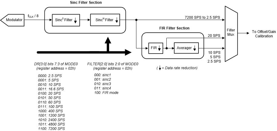
ADS1235 ads1235-digital-filter-block-diagram.gifFigure 48. Digital Filter Block Diagram