ZHCSFP3C August 2016 – June 2017 ADS124S06 , ADS124S08
PRODUCTION DATA.
- 1 特性
- 2 应用
- 3 说明
- 4 修订历史记录
- 5 Device Family Comparison Table
- 6 Pin Configuration and Functions
- 7 Specifications
- 8 Parameter Measurement Information
-
9 Detailed Description
- 9.1 Overview
- 9.2 Functional Block Diagram
- 9.3
Feature Description
- 9.3.1 Multiplexer
- 9.3.2 Low-Noise Programmable Gain Amplifier
- 9.3.3 Voltage Reference
- 9.3.4 Clock Source
- 9.3.5 Delta-Sigma Modulator
- 9.3.6 Digital Filter
- 9.3.7 Excitation Current Sources (IDACs)
- 9.3.8 Bias Voltage Generation
- 9.3.9 System Monitor
- 9.3.10 Status Register
- 9.3.11 General-Purpose Inputs and Outputs (GPIOs)
- 9.3.12 Low-Side Power Switch
- 9.3.13 Cyclic Redundancy Check (CRC)
- 9.3.14 Calibration
- 9.4 Device Functional Modes
- 9.5 Programming
- 9.6
Register Map
- 9.6.1
Configuration Registers
- 9.6.1.1 Device ID Register (address = 00h) [reset = xxh]
- 9.6.1.2 Device Status Register (address = 01h) [reset = 80h]
- 9.6.1.3 Input Multiplexer Register (address = 02h) [reset = 01h]
- 9.6.1.4 Gain Setting Register (address = 03h) [reset = 00h]
- 9.6.1.5 Data Rate Register (address = 04h) [reset = 14h]
- 9.6.1.6 Reference Control Register (address = 05h) [reset = 10h]
- 9.6.1.7 Excitation Current Register 1 (address = 06h) [reset = 00h]
- 9.6.1.8 Excitation Current Register 2 (address = 07h) [reset = FFh]
- 9.6.1.9 Sensor Biasing Register (address = 08h) [reset = 00h]
- 9.6.1.10 System Control Register (address = 09h) [reset = 10h]
- 9.6.1.11 Offset Calibration Register 1 (address = 0Ah) [reset = 00h]
- 9.6.1.12 Offset Calibration Register 2 (address = 0Bh) [reset = 00h]
- 9.6.1.13 Offset Calibration Register 3 (address = 0Ch) [reset = 00h]
- 9.6.1.14 Gain Calibration Register 1 (address = 0Dh) [reset = 00h]
- 9.6.1.15 Gain Calibration Register 2 (address = 0Eh) [reset = 00h]
- 9.6.1.16 Gain Calibration Register 3 (address = 0Fh) [reset = 40h]
- 9.6.1.17 GPIO Data Register (address = 10h) [reset = 00h]
- 9.6.1.18 GPIO Configuration Register (address = 11h) [reset = 00h]
- 9.6.1
Configuration Registers
- 10Application and Implementation
- 11Power Supply Recommendations
- 12Layout
- 13器件和文档支持
- 14机械、封装和可订购信息
封装选项
机械数据 (封装 | 引脚)
散热焊盘机械数据 (封装 | 引脚)
- PBS|32
订购信息
11 Power Supply Recommendations
11.1 Power Supplies
The ADS124S0x requires three power supplies: analog (AVDD, AVSS), digital core (DVDD, DGND), and digital I/O (IOVDD, DGND). The analog power supply can be bipolar (for example, AVDD = 2.5 V, AVSS = –2.5 V) or unipolar (for example, AVDD = 3.3 V, AVSS = 0 V) and is independent of the digital power supplies. DVDD is used to power the digital circuits of the devices. IOVDD sets the digital I/O levels (with the exception of the GPIO levels that are set by the analog supply of AVDD and AVSS). IOVDD must be equal to or larger than DVDD.
11.2 Power-Supply Sequencing
AVDD and DVDD may be powered up in any order. However, IOVDD is recommended to be powered up before or at the same time as DVDD. If DVDD comes up before IOVDD, a reset of the device using the RESET pin or the RESET command may be required.
11.3 Power-On Reset
An internal POR is released after all three supplies exceed approximately 1.65 V. Each supply has an individual POR circuit. A brownout condition on any of the three supplies triggers a reset of the complete device.
11.4 Power-Supply Decoupling
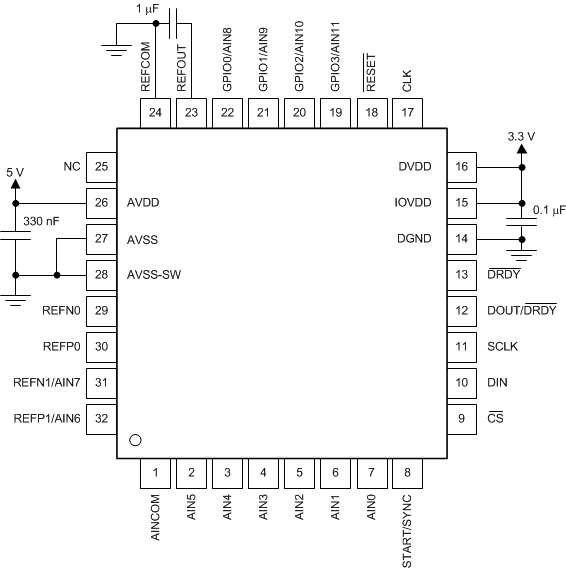
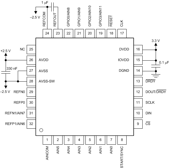
Good power-supply decoupling is important to achieve best performance. AVDD must be decoupled with at least a 330-nF capacitor to AVSS. DVDD and IOVDD (when not connected to DVDD) must be decoupled with at least a 0.1-μF capacitor to DGND. Figure 118 and Figure 119 show typical power-supply decoupling examples for unipolar and bipolar analog supplies, respectively. Place the bypass capacitors as close to the power-supply pins of the device as possible using low-impedance connections. Use multi-layer ceramic chip capacitors (MLCCs) that offer low equivalent series resistance (ESR) and inductance (ESL) characteristics for power-supply decoupling purposes. To reduce inductance on the supply pins, avoid the use of vias for connecting the capacitors to the supply pins. The use of multiple vias in parallel lowers the overall inductance and is beneficial for connections to ground planes. Connect analog and digital grounds together as close to the device as possible.
 Figure 118. Unipolar Analog Power Supply
 Figure 119. Bipolar Analog Power Supply