ZHCSFP3C August 2016 – June 2017 ADS124S06 , ADS124S08
PRODUCTION DATA.
- 1 特性
- 2 应用
- 3 说明
- 4 修订历史记录
- 5 Device Family Comparison Table
- 6 Pin Configuration and Functions
- 7 Specifications
- 8 Parameter Measurement Information
-
9 Detailed Description
- 9.1 Overview
- 9.2 Functional Block Diagram
- 9.3
Feature Description
- 9.3.1 Multiplexer
- 9.3.2 Low-Noise Programmable Gain Amplifier
- 9.3.3 Voltage Reference
- 9.3.4 Clock Source
- 9.3.5 Delta-Sigma Modulator
- 9.3.6 Digital Filter
- 9.3.7 Excitation Current Sources (IDACs)
- 9.3.8 Bias Voltage Generation
- 9.3.9 System Monitor
- 9.3.10 Status Register
- 9.3.11 General-Purpose Inputs and Outputs (GPIOs)
- 9.3.12 Low-Side Power Switch
- 9.3.13 Cyclic Redundancy Check (CRC)
- 9.3.14 Calibration
- 9.4 Device Functional Modes
- 9.5 Programming
- 9.6
Register Map
- 9.6.1
Configuration Registers
- 9.6.1.1 Device ID Register (address = 00h) [reset = xxh]
- 9.6.1.2 Device Status Register (address = 01h) [reset = 80h]
- 9.6.1.3 Input Multiplexer Register (address = 02h) [reset = 01h]
- 9.6.1.4 Gain Setting Register (address = 03h) [reset = 00h]
- 9.6.1.5 Data Rate Register (address = 04h) [reset = 14h]
- 9.6.1.6 Reference Control Register (address = 05h) [reset = 10h]
- 9.6.1.7 Excitation Current Register 1 (address = 06h) [reset = 00h]
- 9.6.1.8 Excitation Current Register 2 (address = 07h) [reset = FFh]
- 9.6.1.9 Sensor Biasing Register (address = 08h) [reset = 00h]
- 9.6.1.10 System Control Register (address = 09h) [reset = 10h]
- 9.6.1.11 Offset Calibration Register 1 (address = 0Ah) [reset = 00h]
- 9.6.1.12 Offset Calibration Register 2 (address = 0Bh) [reset = 00h]
- 9.6.1.13 Offset Calibration Register 3 (address = 0Ch) [reset = 00h]
- 9.6.1.14 Gain Calibration Register 1 (address = 0Dh) [reset = 00h]
- 9.6.1.15 Gain Calibration Register 2 (address = 0Eh) [reset = 00h]
- 9.6.1.16 Gain Calibration Register 3 (address = 0Fh) [reset = 40h]
- 9.6.1.17 GPIO Data Register (address = 10h) [reset = 00h]
- 9.6.1.18 GPIO Configuration Register (address = 11h) [reset = 00h]
- 9.6.1
Configuration Registers
- 10Application and Implementation
- 11Power Supply Recommendations
- 12Layout
- 13器件和文档支持
- 14机械、封装和可订购信息
封装选项
机械数据 (封装 | 引脚)
散热焊盘机械数据 (封装 | 引脚)
- PBS|32
订购信息
12 Layout
12.1 Layout Guidelines
Employing best design practices is recommended when laying out a printed-circuit board (PCB) for both analog and digital components. This recommendation generally means that the layout separates analog components [such as ADCs, amplifiers, references, digital-to-analog converters (DACs), and analog MUXs] from digital components [such as microcontrollers, complex programmable logic devices (CPLDs), field-programmable gate arrays (FPGAs), radio frequency (RF) transceivers, universal serial bus (USB) transceivers, and switching regulators]. An example of good component placement is shown in Figure 120. Although Figure 120 provides a good example of component placement, the best placement for each application is unique to the geometries, components, and PCB fabrication capabilities employed. That is, there is no single layout that is perfect for every design and careful consideration must always be used when designing with any analog component.
 Figure 120. System Component Placement
The following basic recommendations for layout of the ADS124S0x help achieve the best possible performance of the ADC. A good design can be ruined with a bad circuit layout.
- Separate analog and digital signals. To start, partition the board into analog and digital sections where the layout permits. Route digital lines away from analog lines. This prevents digital noise from coupling back into analog signals.
- The ground plane can be split into an analog plane (AGND) and digital plane (DGND), but this (splitting) is not necessary. Place digital signals over the digital plane, and analog signals over the analog plane. As a final step in the layout, the split between the analog and digital grounds must be connected to together at the ADC.
- Fill void areas on signal layers with ground fill.
- Provide good ground return paths. Signal return currents will flow on the path of least impedance. If the ground plane is cut or has other traces that block the current from flowing right next to the signal trace, another path must be found to return to the source and complete the circuit. If forced into a larger path, the chance that the signal radiates increases. Sensitive signals are more susceptible to EMI interference.
- Use bypass capacitors on supplies to reduce high-frequency noise. Do not place vias between bypass capacitors and the active device. Placing the bypass capacitors on the same layer as close to the active device yields the best results.
- Consider the resistance and inductance of the routing. Often, traces for the inputs have resistances that react with the input bias current and cause an added error voltage. Reducing the loop area enclosed by the source signal and the return current reduces the inductance in the path. Reducing the inductance reduces the EMI pickup and reduces the high-frequency impedance at the input of the device.
- Watch for parasitic thermocouples in the layout. Dissimilar metals going from each analog input to the sensor can create a parasitic themocouple that can add an offset to the measurement. Differential inputs must be matched for both the inputs going to the measurement source.
- Analog inputs with differential connections must have a capacitor placed differentially across the inputs. Best input combinations for differential measurements use adjacent analog input lines (such as AIN0, AIN1 and AIN2, AIN3). The differential capacitors must be of high quality. The best ceramic chip capacitors are C0G (NPO) that have stable properties and low noise characteristics.
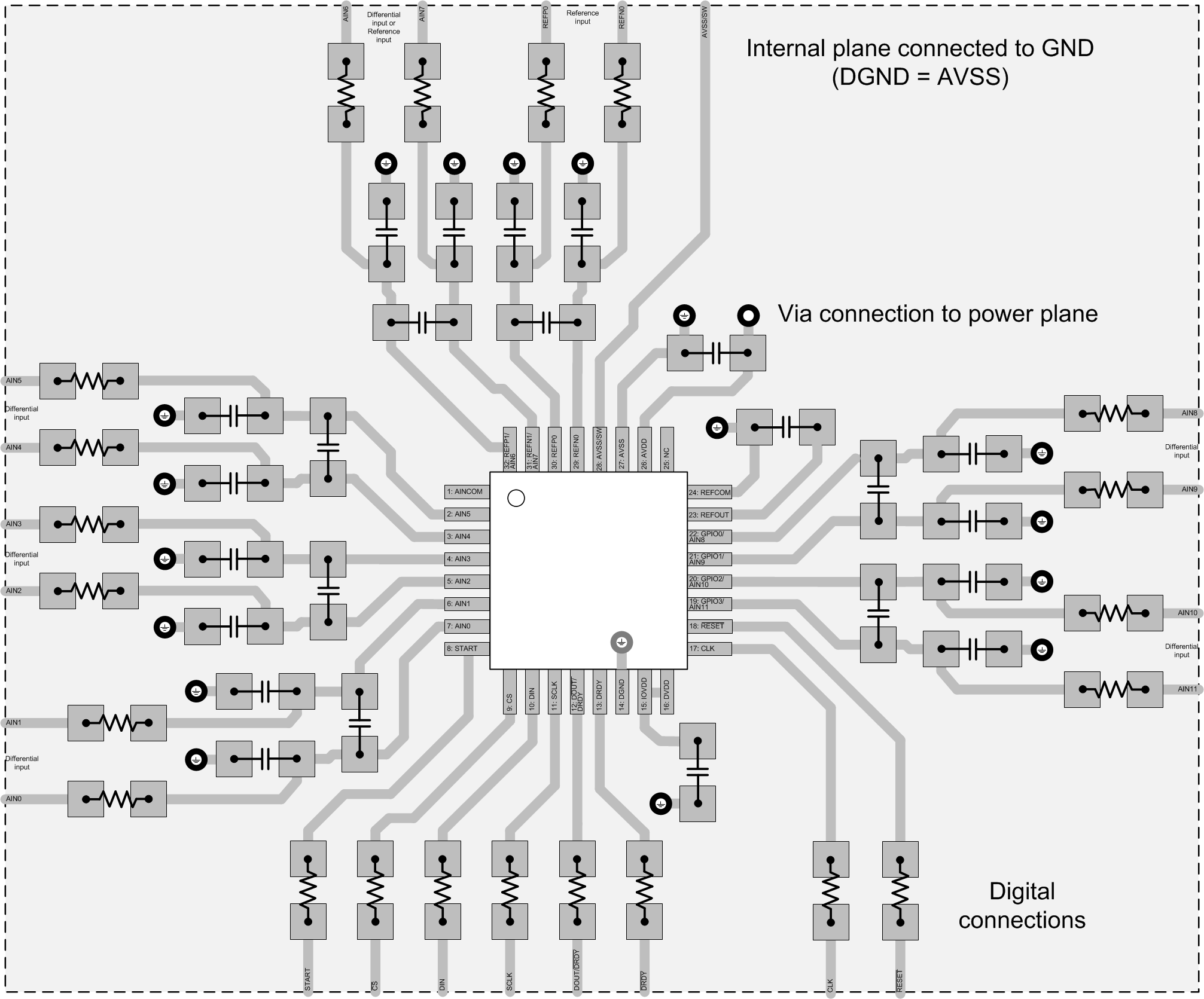
12.2 Layout Example
 Figure 121. ADS124S0x Layout Example