ZHCSFP3C August 2016 – June 2017 ADS124S06 , ADS124S08
PRODUCTION DATA.
- 1 特性
- 2 应用
- 3 说明
- 4 修订历史记录
- 5 Device Family Comparison Table
- 6 Pin Configuration and Functions
- 7 Specifications
- 8 Parameter Measurement Information
-
9 Detailed Description
- 9.1 Overview
- 9.2 Functional Block Diagram
- 9.3
Feature Description
- 9.3.1 Multiplexer
- 9.3.2 Low-Noise Programmable Gain Amplifier
- 9.3.3 Voltage Reference
- 9.3.4 Clock Source
- 9.3.5 Delta-Sigma Modulator
- 9.3.6 Digital Filter
- 9.3.7 Excitation Current Sources (IDACs)
- 9.3.8 Bias Voltage Generation
- 9.3.9 System Monitor
- 9.3.10 Status Register
- 9.3.11 General-Purpose Inputs and Outputs (GPIOs)
- 9.3.12 Low-Side Power Switch
- 9.3.13 Cyclic Redundancy Check (CRC)
- 9.3.14 Calibration
- 9.4 Device Functional Modes
- 9.5 Programming
- 9.6
Register Map
- 9.6.1
Configuration Registers
- 9.6.1.1 Device ID Register (address = 00h) [reset = xxh]
- 9.6.1.2 Device Status Register (address = 01h) [reset = 80h]
- 9.6.1.3 Input Multiplexer Register (address = 02h) [reset = 01h]
- 9.6.1.4 Gain Setting Register (address = 03h) [reset = 00h]
- 9.6.1.5 Data Rate Register (address = 04h) [reset = 14h]
- 9.6.1.6 Reference Control Register (address = 05h) [reset = 10h]
- 9.6.1.7 Excitation Current Register 1 (address = 06h) [reset = 00h]
- 9.6.1.8 Excitation Current Register 2 (address = 07h) [reset = FFh]
- 9.6.1.9 Sensor Biasing Register (address = 08h) [reset = 00h]
- 9.6.1.10 System Control Register (address = 09h) [reset = 10h]
- 9.6.1.11 Offset Calibration Register 1 (address = 0Ah) [reset = 00h]
- 9.6.1.12 Offset Calibration Register 2 (address = 0Bh) [reset = 00h]
- 9.6.1.13 Offset Calibration Register 3 (address = 0Ch) [reset = 00h]
- 9.6.1.14 Gain Calibration Register 1 (address = 0Dh) [reset = 00h]
- 9.6.1.15 Gain Calibration Register 2 (address = 0Eh) [reset = 00h]
- 9.6.1.16 Gain Calibration Register 3 (address = 0Fh) [reset = 40h]
- 9.6.1.17 GPIO Data Register (address = 10h) [reset = 00h]
- 9.6.1.18 GPIO Configuration Register (address = 11h) [reset = 00h]
- 9.6.1
Configuration Registers
- 10Application and Implementation
- 11Power Supply Recommendations
- 12Layout
- 13器件和文档支持
- 14机械、封装和可订购信息
封装选项
机械数据 (封装 | 引脚)
散热焊盘机械数据 (封装 | 引脚)
- PBS|32
订购信息
7 Specifications
7.1 Absolute Maximum Ratings(1)
| MIN | MAX | UNIT | ||
|---|---|---|---|---|
| Power-supply voltage | AVDD to AVSS | –0.3 | 5.5 | V |
| AVSS to DGND | –2.8 | 0.3 | ||
| DVDD to DGND | –0.3 | 3.9 | ||
| IOVDD to DGND | –0.3 | 5.5 | ||
| Analog input voltage | AINx, GPIOx, REFPx, REFNx, REFCOM | AVSS – 0.3 | AVDD + 0.3 | V |
| Digital input voltage | CS, SCLK, DIN, DOUT/DRDY, DRDY, START, RESET, CLK |
DGND – 0.3 | IOVDD + 0.3 | V |
| Input current | Continuous, AVSS-SW, REFN0, REFOUT | –100 | 100 | mA |
| Continuous, all other pins except power-supply pins | –10 | 10 | ||
| Temperature | Junction, TJ | 150 | °C | |
| Storage, Tstg | –60 | 150 | ||
(1) Stresses beyond those listed under Absolute Maximum Ratings may cause permanent damage to the device. These are stress ratings only, which do not imply functional operation of the device at these or any other conditions beyond those indicated under Recommended Operating Conditions. Exposure to absolute-maximum-rated conditions for extended periods may affect device reliability.
7.2 ESD Ratings
| VALUE | UNIT | |||
|---|---|---|---|---|
| V(ESD) | Electrostatic discharge | Human-body model (HBM), per ANSI/ESDA/JEDEC JS-001(1) | ±2500 | V |
| Charged-device model (CDM), per JEDEC specification JESD22-C101(2) | ±1000 | |||
(1) JEDEC document JEP155 states that 500-V HBM allows safe manufacturing with a standard ESD control process.
(2) JEDEC document JEP157 states that 250-V CDM allows safe manufacturing with a standard ESD control process.
7.3 Recommended Operating Conditions
over operating ambient temperature range (unless otherwise noted)| MIN | NOM | MAX | UNIT | |||
|---|---|---|---|---|---|---|
| POWER SUPPLY | ||||||
| Analog power supply | AVDD to AVSS | 2.7 | 5.25 | V | ||
| AVSS to DGND | –2.625 | 0 | 0.05 | |||
| AVDD to DGND | 1.5 | 5.25 | ||||
| Digital core power supply | DVDD to DGND | 2.7 | 3.6 | V | ||
| Digital IO power supply | IOVDD to DGND | DVDD | 5.25 | V | ||
| ANALOG INPUTS(1) | ||||||
| V(AINx) | Absolute input voltage(2) | PGA bypassed | AVSS – 0.05 | AVDD + 0.05 | V | |
| PGA enabled, gain = 1 to 16 | AVSS + 0.15 + |VINMAX|·(Gain – 1) / 2 | AVDD – 0.15 – |VINMAX|·(Gain –1) / 2 | ||||
| PGA enabled, gain = 32 to 128 | AVSS + 0.15 + 15.5·|VINMAX| | AVDD – 0.15 – 15.5·|VINMAX| | ||||
| VIN | Differential input voltage | VIN = VAINP – VAINN | –VREF / Gain | VREF / Gain | V | |
| VOLTAGE REFERENCE INPUTS(3) | ||||||
| VREF | Differential reference input voltage | VREF = V(REFPx) – V(REFNx) | 0.5 | AVDD – AVSS | V | |
| V(REFNx) | Absolute negative reference voltage | Negative reference buffer disabled | AVSS – 0.05 | V(REFPx) – 0.5 | V | |
| Negative reference buffer enabled | AVSS | V(REFPx) – 0.5 | V | |||
| V(REFPx) | Absolute positive reference voltage | Positive reference buffer disabled | V(REFNx) + 0.5 | AVDD + 0.05 | V | |
| Positive reference buffer enabled | V(REFNx) + 0.5 | AVDD | V | |||
| EXTERNAL CLOCK SOURCE(4) | ||||||
| fCLK | External clock frequency | 2 | 4.096 | 4.5 | MHz | |
| Duty cycle | 40% | 50% | 60% | |||
| GENERAL-PURPOSE INPUTS (GPIOs) | ||||||
| Input voltage | AVSS – 0.05 | AVDD + 0.05 | V | |||
| DIGITAL INPUTS (Other than GPIOs) | ||||||
| Input voltage | DGND | IOVDD | V | |||
| TEMPERATURE RANGE | ||||||
| TA | Operating ambient temperature | –50 | 125 | °C | ||
(1) AINP and AINN denote the positive and negative inputs of the PGA. Any of the available analog inputs (AINx) can be selected as either AINP or AINN by the input multiplexer.
(2) VINMAX denotes the maximum differential input voltage, VIN, that is expected in the application. |VINMAX| can be smaller than VREF / Gain.
(3) REFPx and REFNx denote one of the two available external differential reference input pairs.
(4) An external clock is not required when the internal oscillator is used.
7.4 Thermal Information
| THERMAL METRIC(1) | ADS124S06, ADS124S08 | UNIT | ||
|---|---|---|---|---|
| VQFN (RHB) | TQFP (PBS) | |||
| 32 PINS | 32 PINS | |||
| RθJA | Junction-to-ambient thermal resistance | 45.2 | 75.5 | °C/W |
| RθJC(top) | Junction-to-case (top) thermal resistance | 28.3 | 17.1 | °C/W |
| RθJB | Junction-to-board thermal resistance | 15.8 | 28.5 | °C/W |
| ψJT | Junction-to-top characterization parameter | 0.4 | 0.4 | °C/W |
| ψJB | Junction-to-board characterization parameter | 15.7 | 28.3 | °C/W |
| RθJC(bot) | Junction-to-case (bottom) thermal resistance | 2.3 | n/a | °C/W |
(1) For more information about traditional and new thermal metrics, see the Semiconductor and IC Package Thermal Metrics application report.
7.5 Electrical Characteristics
minimum and maximum specifications apply from TA = –50°C to +125°C; Typical specifications are at TA = 25°C;all specifications are at AVDD = 2.7 V to 5.25 V, AVSS = 0 V, DVDD = IOVDD = 3.3 V, all gains, internal reference, internal oscillator, all data rates, and global chop disabled (unless otherwise noted)
| PARAMETER | TEST CONDITIONS | MIN | TYP | MAX | UNIT | |||
|---|---|---|---|---|---|---|---|---|
| ANALOG INPUTS | ||||||||
| Absolute input current | PGA bypassed, AVSS + 0.1 V ≤ V(AINx) ≤ AVDD – 0.1 V |
0.5 | nA | |||||
| PGA enabled, all gains, V(AINx)MIN ≤ V(AINx) ≤ V(AINx)MAX |
–2 | 0.1 | 2 | |||||
| Absolute input current drift | PGA bypassed, AVSS + 0.1 V ≤ V(AINx) ≤ AVDD – 0.1 V |
2 | pA/°C | |||||
| PGA enabled, all gains, V(AINx)MIN ≤ V(AINx) ≤ V(AINx)MAX |
2 | |||||||
| Differential input current | PGA bypassed, VCM = AVDD / 2, –VREF ≤ VIN ≤ VREF |
1 | nA/V | |||||
| PGA enabled, all gains, VCM = AVDD / 2, –VREF / Gain ≤ VIN ≤ VREF / Gain |
–1 | 0.02 | 1 | nA | ||||
| Differential input current drift | PGA bypassed, VCM = AVDD / 2, –VREF ≤ VIN ≤ VREF |
3 | pA/°C | |||||
| PGA enabled, all gains, VCM = AVDD / 2, –VREF / Gain ≤ VIN ≤ VREF / Gain |
1 | |||||||
| PGA | ||||||||
| Gain settings | 1, 2, 4, 8, 16, 32, 64, 128 |
|||||||
| Startup time | Enabling the PGA in conversion mode | 190 | µs | |||||
| SYSTEM PERFORMANCE | ||||||||
| Resolution (no missing codes) | 24 | Bits | ||||||
| DR | Data rate | 2.5, 5, 10, 16.6, 20, 50, 60, 100, 200, 400, 800, 1000, 2000, 4000 |
SPS | |||||
| INL | Integral nonlinearity (best fit) | PGA bypassed, VCM = AVDD / 2 | 1 | 10 | ppmFSR | |||
| PGA enabled, gain = 1 to 8, VCM = AVDD / 2 | 2 | 15 | ||||||
| PGA enabled, gain = 16 to 128, VCM = AVDD / 2, TA = –40°C to +85°C |
3 | 15 | ||||||
| VIO | Input offset voltage | TA = 25°C, PGA bypassed | –120 | 20 | 120 | µV | ||
| TA = 25°C, PGA enabled, gain = 1 to 8 | –120 / Gain | 20 / Gain | 120 / Gain | |||||
| TA = 25°C, PGA enabled, gain = 16 to 128 | –15 | 2 | 15 | |||||
| TA = 25°C, PGA bypassed, after internal offset calibration | On the order of noisePP at the set DR and gain | |||||||
| TA = 25°C, PGA enabled, gain = 1 to 128, after internal offset calibration | On the order of noisePP at the set DR and gain | |||||||
| TA = 25°C, PGA bypassed, global chop enabled | –2 | 0.2 | 2 | |||||
| TA = 25°C, PGA enabled, gain = 1 to 128, global chop enabled |
–2 | 0.2 | 2 | |||||
| Offset drift | TA = –40°C to +85°C, PGA bypassed | –75 | 10 | 75 | nV/°C | |||
| TA = –40°C to +85°C, PGA enabled, gain = 1 to 128 | –100 | 15 | 100 | |||||
| PGA bypassed | –75 | 10 | 75 | |||||
| PGA enabled, gain = 1 to 8 | –200 | 15 | 200 | |||||
| PGA enabled, gain = 16 to 128 | –150 | 15 | 150 | |||||
| PGA bypassed, global chop enabled | –10 | 2 | 10 | |||||
| PGA enabled, gain = 1 to 128, global chop enabled | –10 | 2 | 10 | |||||
| SYSTEM PERFORMANCE (continued) | ||||||||
| Gain error(1) | TA = 25°C, PGA bypassed | 40 | 120 | ppm | ||||
| TA = 25°C, PGA enabled, gain = 1 to 32 | 40 | 120 | ||||||
| TA = 25°C, PGA enabled, gain = 64 and 128 | 40 | 200 | ||||||
| Gain drift(1) | TA = –40°C to +85°C, PGA bypassed | 0.5 | 1 | ppm/°C | ||||
| TA = –40°C to +85°C, PGA enabled, gain = 1 to 128 | 0.5 | 2 | ||||||
| PGA bypassed | 0.5 | 1 | ||||||
| PGA enabled, gain = 1 to 128 | 1 | 4 | ||||||
| Noise (input-referred)(2) | PGA enabled, gain = 128, DR = 2.5 SPS, sinc3 filter |
19 | nVRMS | |||||
| NMRR | Normal-mode rejection ratio(3) | fIN = 50 Hz or 60 Hz (±1 Hz), DR = 10 SPS, sinc3 filter |
88 | dB | ||||
| fIN = 50 Hz or 60 Hz (±1 Hz), DR = 10 SPS, sinc3 filter, external fCLK = 4.096 MHz |
102 | |||||||
| fIN = 50 Hz or 60 Hz (±1 Hz), DR = 20 SPS, low-latency filter |
79 | |||||||
| fIN = 50 Hz or 60 Hz (±1 Hz), DR = 20 SPS, low-latency filter, external fCLK = 4.096 MHz |
95 | |||||||
| fIN = 50 Hz (±1 Hz), DR = 50 SPS, sinc3 filter | 87 | |||||||
| fIN = 50 Hz (±1 Hz), DR = 50 SPS, sinc3 filter, external fCLK = 4.096 MHz |
101 | |||||||
| fIN = 60 Hz (±1 Hz), DR = 60 SPS, sinc3 filter | 89 | |||||||
| fIN = 60 Hz (±1 Hz), DR = 60 SPS, sinc3 filter, external fCLK = 4.096 MHz |
105 | |||||||
| CMRR | Common-mode rejection ratio | At dc | 110 | 120 | dB | |||
| fCM = 50 Hz or 60 Hz (±1 Hz), DR = 2.5 SPS to 10 SPS, sinc3 filter |
120 | 130 | ||||||
| fCM = 50 Hz or 60 Hz (±1 Hz), DR = 2.5 SPS, 5 SPS, 10 SPS, 20 SPS, low-latency filter |
115 | 125 | ||||||
| PSRR | Power-supply rejection ratio | AVDD at dc | 90 | 105 | dB | |||
| AVDD at 50 Hz or 60 Hz | 100 | 115 | ||||||
| DVDD at dc | 100 | 115 | ||||||
| VOLTAGE REFERENCE INPUTS | ||||||||
| Absolute input current | Reference buffers disabled, external VREF = 2.5 V, REFP1/REFN1 inputs |
-6 | 4 | 6 | µA/V | |||
| Reference buffers enabled, external VREF = 2.5 V, REFP1/REFN1 inputs |
–15 | 5 | 15 | nA | ||||
| INTERNAL VOLTAGE REFERENCE | ||||||||
| VREF | Output voltage | 2.5 | V | |||||
| Accuracy | TA = 25°C, TQFP package | –0.05% | ±0.01% | 0.05% | ||||
| TA = 25°C, VQFN package | –0.1% | ±0.01% | 0.1% | |||||
| Temperature drift | TA = –40°C to +85°C | 2.5 | 8 | ppm/°C | ||||
| TA = –50°C to +125°C | 3 | 10 | ||||||
| Output current | AVDD = 2.7 V to 3.3 V, sink and source | –5 | 5 | mA | ||||
| AVDD = 3.3 V to 5.25 V, sink and source | –10 | 10 | ||||||
| Short-circuit current limit | Sink and source | 70 | 100 | mA | ||||
| PSRR | Power-supply rejection ratio | AVDD at dc | 85 | dB | ||||
| Load regulation | AVDD = 2.7 V to 3.3 V, load current = –5 mA to 5 mA |
8 | µV/mA | |||||
| AVDD = 3.3 V to 5.25 V, load current = –10 mA to 10 mA |
8 | |||||||
| Startup time | 1-µF capacitor on REFOUT, 0.001% settling | 5.9 | ms | |||||
| Capacitive load stability | Capacitor on REFOUT | 1 | 47 | µF | ||||
| Reference noise | f = 0.1 Hz to 10 Hz, 1-µF capacitor on REFOUT | 9 | µVPP | |||||
| INTERNAL OSCILLATOR | ||||||||
| fCLK | Frequency | 4.096 | MHz | |||||
| Accuracy | –1.5% | 1.5% | ||||||
| EXCITATION CURRENT SOURCES (IDACS) | ||||||||
| Current settings | 10, 50, 100, 250, 500, 750, 1000, 1500, 2000 |
µA | ||||||
| Compliance voltage(4) | 10 µA to 750 µA, 0.1% deviation | AVSS | AVDD – 0.4 | V | ||||
| 1 mA to 2 mA, 0.1% deviation | AVSS | AVDD – 0.6 | ||||||
| Accuracy (each IDAC) | TA = 25°C, 10 µA to 100 µA | –5% | ±0.7% | 5% | ||||
| TA = 25°C, 250 µA to 2 mA | –3% | ±0.5% | 3% | |||||
| Current mismatch between IDACs | TA = 25°C, 10 µA to 100 µA | 0.15% | 0.8% | |||||
| TA = 25°C, 250 µA to 750 µA | 0.10% | 0.6% | ||||||
| TA = 25°C, 1 mA to 2 mA | 0.07% | 0.4% | ||||||
| Temperature drift (each IDAC) | 10 µA to 750 µA | 20 | 120 | ppm/°C | ||||
| 1 mA to 2 mA | 10 | 80 | ||||||
| Temperature drift matching between IDACs | 10 µA to 100 µA | 3 | 25 | ppm/°C | ||||
| 250 µA to 2 mA | 2 | 15 | ||||||
| Startup time | With internal reference already settled. From end of WREG command to current flowing out of pin. | 22 | µs | |||||
| BIAS VOLTAGE | ||||||||
| VBIAS | Output voltage settings | (AVDD + AVSS) / 2, (AVDD + AVSS) / 12 |
V | |||||
| Output impedance | 350 | Ω | ||||||
| Startup time | Combined capacitive load on all selected analog inputs CLOAD = 1 µF, 0.1% settling | 2.8 | ms | |||||
| BURNOUT CURRENT SOURCES (BOCS) | ||||||||
| Current settings | 0.2, 1, 10 | µA | ||||||
| Accuracy | 0.2 µA, sinking or sourcing | ±8% | ||||||
| 1 µA, sinking or sourcing | ±4% | |||||||
| 10 µA, sinking or sourcing | ±2% | |||||||
| PGA RAIL DETECTION | ||||||||
| Positive rail threshold | Referred to the output of the PGA | AVDD – 0.15 | V | |||||
| Negative rail threshold | Referred to the output of the PGA | AVSS + 0.15 | V | |||||
| REFERENCE DETECTION | ||||||||
| Threshold 1 | 0.3 | V | ||||||
| Threshold 2 | 1/3·(AVDD – AVSS) | V | ||||||
| Threshold 2 accuracy | –3% | ±1% | 3% | |||||
| Pull-together resistance | 10 | MΩ | ||||||
| SUPPLY VOLTAGE MONITORS | ||||||||
| Accuracy | (AVDD – AVSS) / 4 monitor | ±1% | ||||||
| DVDD / 4 monitor | ±1% | |||||||
| TEMPERATURE SENSOR | ||||||||
| Output voltage | TA = 25°C | 129 | mV | |||||
| Temperature coefficient | 403 | µV/°C | ||||||
| LOW-SIDE POWER SWITCH | ||||||||
| RON | On-resistance | 1 | 3 | Ω | ||||
| Current through switch | 75 | mA | ||||||
| GENERAL-PURPOSE INPUT/OUTPUTS (GPIOs) | ||||||||
| VIL | Logic input level, low | AVSS – 0.05 | 0.3 AVDD | V | ||||
| VIH | Logic input level, high | 0.7 AVDD | AVDD + 0.05 | V | ||||
| VOL | Logic output level, low | IOL = 1 mA | AVSS | 0.2 AVDD | V | |||
| VOH | Logic output level, high | IOH = 1 mA | 0.8 AVDD | AVDD | V | |||
| DIGITAL INPUT/OUTPUTS | ||||||||
| VIL | Logic input level, low | DGND | 0.3 IOVDD | V | ||||
| VIH | Logic input level, high | 0.7 IOVDD | IOVDD | V | ||||
| VOL | Logic output level, low | IOL = 1 mA | DGND | 0.2 IOVDD | V | |||
| VOH | Logic output level, high | IOH = 1 mA | 0.8 IOVDD | IOVDD | V | |||
| Input current | DGND ≤ VDigital Input ≤ IOVDD | –1 | 1 | µA | ||||
| ANALOG SUPPLY CURRENT (AVDD = 3.3 V, External Reference, Internal Reference Disabled, Reference Buffers Disabled, IDACs Disabled, VBIAS Disabled, Flags Disabled, Internal Oscillator, All Data Rates, VIN = 0 V) | ||||||||
| IAVDD | Analog supply current | Power-down mode | 0.1 | 1.5 | µA | |||
| Standby mode, PGA bypassed | 70 | |||||||
| Conversion mode, PGA bypassed | 85 | |||||||
| Conversion mode, PGA enabled, gain = 1, 2 | 120 | 135 | ||||||
| Conversion mode, PGA enabled, gain = 4, 8 | 140 | 155 | ||||||
| Conversion mode, PGA enabled, gain = 16, 32 | 165 | 180 | ||||||
| Conversion mode, PGA enabled, gain = 64 | 200 | |||||||
| Conversion mode, PGA enabled, gain = 128 | 250 | |||||||
| ADDITIONAL ANALOG SUPPLY CURRENTS PER FUNCTION (AVDD = 3.3 V) | ||||||||
| IAVDD | Analog supply current | Internal 2.5-V reference, no external load | 185 | 280 | µA | |||
| Positive reference buffer | 35 | 60 | ||||||
| Negative reference buffer | 25 | 40 | ||||||
| VBIAS buffer, no external load | 10 | |||||||
| IDAC overhead, 10 µA to 250 µA | 20 | 35 | ||||||
| IDAC overhead, 500 µA to 750 µA | 30 | |||||||
| IDAC overhead, 1 mA | 40 | |||||||
| IDAC overhead, 1.5 mA | 50 | |||||||
| IDAC overhead, 2 mA | 65 | |||||||
| PGA rail detection and reference detection circuit | 10 | |||||||
| DIGITAL SUPPLY CURRENT (DVDD = IOVDD = 3.3 V, All Data Rates, SPI Not Active) | ||||||||
| IDVDD + IIOVDD | Digital supply current | Power-down mode, internal oscillator | 0.1 | µA | ||||
| Standby mode, internal oscillator | 185 | |||||||
| Conversion mode, internal oscillator | 225 | 300 | ||||||
| Conversion mode, external fCLK = 4.096 MHz | 195 | |||||||
| POWER DISSIPATION (AVDD = DVDD = IOVDD = 3.3 V, Internal Reference Enabled, Reference Buffers Disabled, IDACs Disabled, VBIAS Disabled, Flags Disabled, Internal Oscillator, All Data Rates, VIN = 0 V, SPI Not Active) | ||||||||
| PD | Power dissipation | Conversion mode, PGA enabled, gain = 1 | 1.75 | mW | ||||
(1) Excluding error of voltage reference.
(2) See the Noise Performance section for more information.
(3) See the 50-Hz and 60-Hz Line Cycle Rejection section for more information.
(4) The IDAC current does not change by more than 0.1% from the nominal value when staying within the specified compliance voltage.
7.6 Timing Characteristics
over operating ambient temperature range, DVDD = 2.7 V to 3.6 V, IOVDD = DVDD to 5.25 V, andDOUT/DRDY load = 20 pF || 100 kΩ to DGND (unless otherwise noted)
| MIN | MAX | UNIT(1) | ||
|---|---|---|---|---|
| SERIAL INTERFACE | ||||
| td(CSSC) | Delay time, first SCLK rising edge after CS falling edge | 20 | ns | |
| td(SCCS) | Delay time, CS rising edge after final SCLK falling edge | 20 | ns | |
| tw(CSH) | Pulse duration, CS high | 30 | ns | |
| tc(SC) | SCLK period | 100 | ns | |
| tw(SCH) | Pulse duration, SCLK high | 40 | ns | |
| tw(SCL) | Pulse duration, SCLK low | 40 | ns | |
| tsu(DI) | Setup time, DIN valid before SCLK falling edge | 15 | ns | |
| th(DI) | Hold time, DIN valid after SCLK falling edge | 20 | ns | |
| td(CMD) | Delay time, between bytes or commands | 0 | ns | |
| RESET PIN | ||||
| tw(RSL) | Pulse duration, RESET low | 4 | tCLK | |
| td(RSSC) | Delay time, first SCLK rising edge after RESET rising edge (or 7th SCLK falling edge of RESET command) | 4096 | tCLK | |
| START/SYNC PIN | ||||
| tw(STH) | Pulse duration, START/SYNC high | 4 | tCLK | |
| tw(STL) | Pulse duration, START/SYNC low | 4 | tCLK | |
| tsu(STDR) | Setup time, START/SYNC falling edge (or 7th SCLK falling edge of STOP command) before DRDY falling edge to stop further conversions (continuous conversion mode) | 32 | tCLK | |
| READING CONVERSION DATA WITHOUT RDATA COMMAND | ||||
| th(SCDR) | Hold time, SCLK low before DRDY falling edge(2) | 28 | tCLK | |
| td(DRSC) | Delay time, SCLK rising edge after DRDY falling edge(2) | 4 | tCLK | |
(1) tCLK = 1 / fCLK.
(2) Only applicable when reading data without the RDATA command. All commands can be send without any SCLK to DRDY signal timing restrictions.
7.7 Switching Characteristics
over operating ambient temperature range, DVDD = 2.7 V to 3.6 V, IOVDD = DVDD to 5.25 V, andDOUT/DRDY load = 20 pF || 100 kΩ to DGND (unless otherwise noted)
| PARAMETER | TEST CONDITIONS | MIN | TYP | MAX | UNIT(1) | |
|---|---|---|---|---|---|---|
| tp(CSDO) | Propagation delay time, CS falling edge to DOUT driven | 0 | 25 | ns | ||
| tp(SCDO) | Propagation delay time, SCLK rising edge to valid new DOUT | 3 | 30 | ns | ||
| tp(CSDOZ) | Propagation delay time, CS rising edge to DOUT high impedance | 0 | 25 | ns | ||
| tp(STDR) | Propagation delay time, START/SYNC rising edge (or first SCLK rising edge of any command or data read) to DRDY rising edge | 2 | tCLK | |||
| tw(DRH) | Pulse duration, DRDY high | 24 | tCLK | |||
| tp(GPIO) | Propagation delay time, last SCLK falling edge of WREG command to GPIOx output valid | 3 | 100 | ns | ||
| SPI timeout per 8 bit(2) | 215 | tCLK | ||||
(1) tCLK = 1 / fCLK
(2) The SPI interface resets when an entire byte is not sent within the specified timeout time.

NOTE:
Single-byte communication is shown. Actual communication can be multiple bytes.
NOTE:
Single-byte communication is shown. Actual communication can be multiple bytes. Figure 3. RESET Pin and RESET Command Timing Requirements
 Figure 4. START/SYNC Pin Timing Requirements
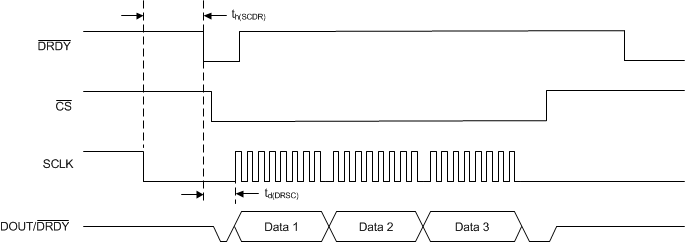 Figure 6. Read Data Direct (Without an RDATA Command) Timing Requirements
 Figure 7. GPIO Switching Characteristics
7.8 Typical Characteristics
at TA = 25°C, AVDD = 3.3 V, AVSS = 0 V, DVDD = IOVDD = 3.3 V, using internal VREF = 2.5 V, internal 4.096-MHz oscillator, and PGA enabled (unless otherwise noted)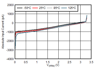
| PGA bypassed, DR = 20 SPS, VIN = 0 V |
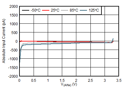
| PGA enabled, gain = 1, DR = 20 SPS, VIN = 0 V |
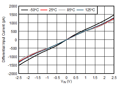
| PGA bypassed, DR = 20 SPS, VCM = 1.65 V |
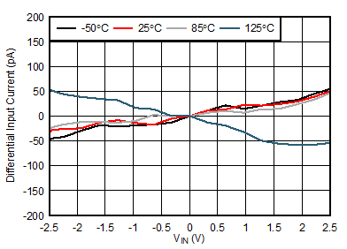
| PGA enabled, DR = 20 SPS, VCM = 1.65 V |
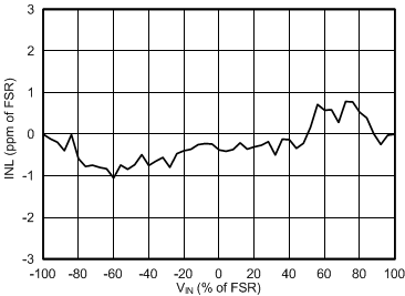
| PGA bypassed, gain = 1 |

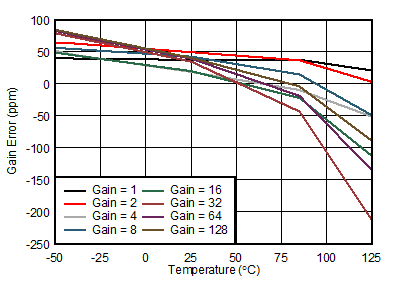


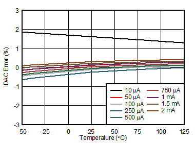
| IDAC output voltage = 1.65 V |
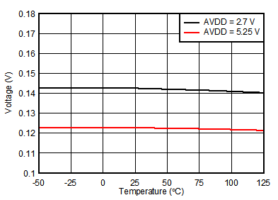
![ADS124S06 ADS124S08 VBIAS Voltage [(AVDD –
AVSS) / 2] vs Temperature ADS124S06 ADS124S08 D034_sbas660.gif](/ods/images/ZHCSFP3C/D034_sbas660.gif)
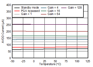
| Level 0 = 300 mV |


| AVDD = 3.3 V |

| DVDD = 3.3 V |
| Standby and conversion mode, external VREF |

| Power-down mode |
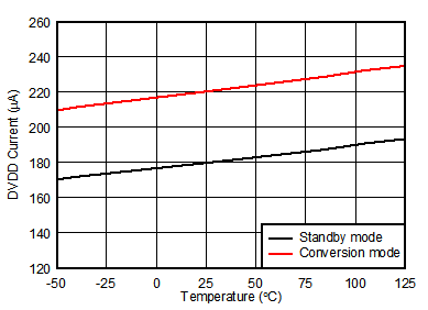
| Standby and conversion mode |
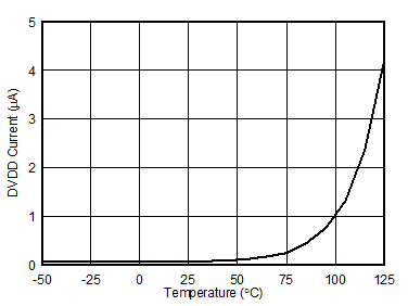
| Power-down mode |

| PGA bypassed, DR = 4 kSPS, VIN = 0 V |

| PGA enabled, gain = 1, DR = 4 kSPS, VIN = 0 V |
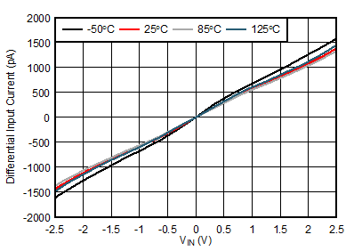
| PGA bypassed, DR = 4 kSPS, VCM = 1.65 V |
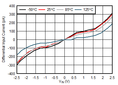
| PGA enabled, DR = 4 kSPS, VCM = 1.65 V |
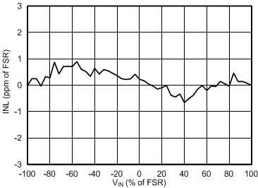
| PGA enabled, gain = 1 |
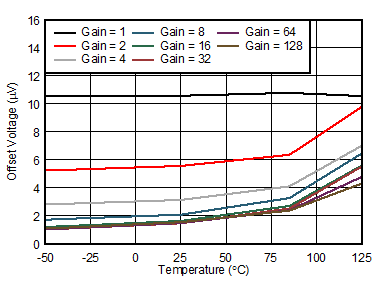
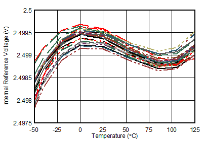
| 28 units, TQFP package |
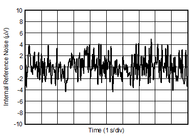
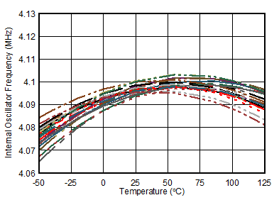
| 28 units | ||

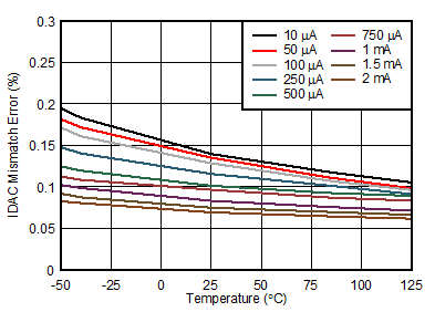
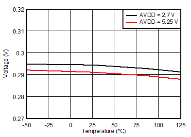
![ADS124S06 ADS124S08 VBIAS Voltage [(AVDD –
AVSS) / 12] vs Temperature ADS124S06 ADS124S08 D035_sbas660.gif](/ods/images/ZHCSFP3C/D035_sbas660.gif)
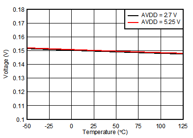

| Level 1 = 1/3 · (AVDD – AVSS) |

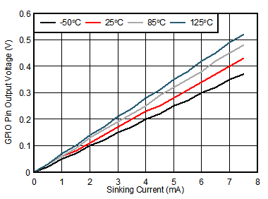
| AVDD = 3.3 V |

| DVDD = 3.3 V |
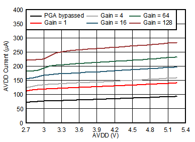
| Conversion mode, external VREF |
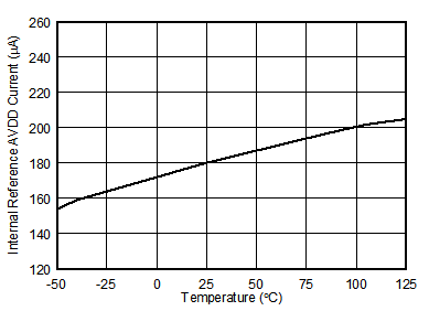
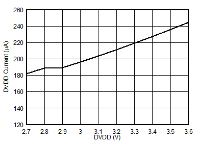
| Conversion mode |
