ZHCSEA6B September 2015 – April 2016 ADS1257
PRODUCTION DATA.
- 1 特性
- 2 应用
- 3 说明
- 4 修订历史记录
- 5 Device Comparison Table
- 6 Pin Configuration and Functions
-
7 Specifications
- 7.1 Absolute Maximum Ratings
- 7.2 ESD Ratings
- 7.3 Recommended Operating Conditions
- 7.4 Thermal Information
- 7.5 Electrical Characteristics
- 7.6 Serial Interface Timing Requirements
- 7.7 Serial Interface Switching Characteristics
- 7.8 RESET and SYNC/PWDN Timing Requirements
- 7.9 SCLK Reset Timing Requirements
- 7.10 DRDY Update Timing Characteristics
- 7.11 Typical Characteristics
- 8 Parameter Measurement Information
-
9 Detailed Description
- 9.1 Overview
- 9.2 Functional Block Diagram
- 9.3
Feature Description
- 9.3.1 Input Multiplexer
- 9.3.2 Analog Input Buffer
- 9.3.3 Programmable Gain Amplifier (PGA)
- 9.3.4 Modulator Input Circuitry
- 9.3.5 Voltage Reference Inputs (REFP, REFN)
- 9.3.6 Clock Input (CLKIN)
- 9.3.7 Clock Output (D0/CLKOUT)
- 9.3.8 General-Purpose Digital I/O (D0, D1)
- 9.3.9 Open- and Short-Circuit Sensor Detection
- 9.3.10 Digital Filter
- 9.4 Device Functional Modes
- 9.5
Programming
- 9.5.1 Serial Interface
- 9.5.2 Data Format
- 9.5.3
Command Definitions
- 9.5.3.1 WAKEUP/NOP: Complete Synchronization or Exit Standby Mode
- 9.5.3.2 RDATA: Read Data
- 9.5.3.3 RDATAC: Read Data Continuous
- 9.5.3.4 SDATAC: Stop Read Data Continuous
- 9.5.3.5 RREG: Read from Registers
- 9.5.3.6 WREG: Write to Register
- 9.5.3.7 SELFCAL: Self-Offset and Self-Gain Calibration
- 9.5.3.8 SELFOCAL: Self Offset Calibration
- 9.5.3.9 SELFGCAL: Self Gain Calibration
- 9.5.3.10 SYSOCAL: System Offset Calibration
- 9.5.3.11 SYSGCAL: System Gain Calibration
- 9.5.3.12 STANDBY: Standby Mode / Single-shot Mode
- 9.5.3.13 RESET: Reset Registers to Default Values
- 9.5.3.14 SYNC: Synchronize the Analog-to-Digital Conversion
- 9.6
Register Map
- 9.6.1 STATUS: Status Register (address = 00h) [reset = x1h]
- 9.6.2 MUX : Input Multiplexer Control Register (address = 01h) [reset = 01h]
- 9.6.3 ADCON: ADC Control Register (address = 02h) [reset = 20h]
- 9.6.4 DRATE: ADC Data Rate Register (address = 03h) [reset = F0h]
- 9.6.5 IO: GPIO Control Register (address = 04h) [reset = E0h]
- 9.6.6 OFC0: Offset Calibration Register 0 (address = 05h) [reset = depends on calibration results]
- 9.6.7 OFC1: Offset Calibration Register 1 (address = 06h) [reset = depends on calibration results]
- 9.6.8 OFC2: Offset Calibration Register 2 (address = 07h) [reset = depends on calibration results]
- 9.6.9 FSC0: Full-Scale Calibration Register 0 (address = 08h) [reset = depends on calibration results]
- 9.6.10 FSC1: Full-Scale Calibration Register 1 (address = 09h) [reset = depends on calibration results]
- 9.6.11 FSC2: Full-Scale Calibration Register 2 (address = 0Ah) [reset = depends on calibration results]
- 10Applications and Implementation
- 11Power Supply Recommendations
- 12Layout
- 13器件和文档支持
- 14机械、封装和可订购信息
7 Specifications
7.1 Absolute Maximum Ratings(1)
| MIN | MAX | UNIT | ||
|---|---|---|---|---|
| Power-supply voltage | AVDD to AGND | –0.3 | 6.0 | V |
| DVDD to DGND | –0.3 | 3.6 | ||
| Analog input voltage | AINx, REFP, REFN | AGND – 0.3 | AVDD + 0.3 | V |
| Digital input voltage | DIN, SCLK, CS, RESET, SYNC/PWDN, CLKIN | DGND – 0.3 | DGND + 6.0 | V |
| D0/CLKOUT, D1 | DGND – 0.3 | DVDD + 0.3 | ||
| Input current | Continuous, any pins except power-supply pins | –10 | 10 | mA |
| Temperature | Operating ambient, TA | –40 | 105 | °C |
| Junction, TJ | –40 | 150 | ||
| Storage, Tstg | –60 | 150 | ||
(1) Stresses beyond those listed under Absolute Maximum Ratings may cause permanent damage to the device. These are stress ratings only, which do not imply functional operation of the device at these or any other conditions beyond those indicated under Recommended Operating Conditions. Exposure to absolute-maximum-rated conditions for extended periods may affect device reliability.
7.2 ESD Ratings
| VALUE | UNIT | |||
|---|---|---|---|---|
| V(ESD) | Electrostatic discharge | Human-body model (HBM), per ANSI/ESDA/JEDEC JS-001(1) | ±2000 | V |
| Charged-device model (CDM), per JEDEC specification JESD22-C101(2) | ±500 | |||
(1) JEDEC document JEP155 states that 500-V HBM allows safe manufacturing with a standard ESD control process.
(2) JEDEC document JEP157 states that 250-V CDM allows safe manufacturing with a standard ESD control process.
7.3 Recommended Operating Conditions
over operating ambient temperature range (unless otherwise noted)| MIN | NOM | MAX | UNIT | |||
|---|---|---|---|---|---|---|
| POWER SUPPLY | ||||||
| Analog power supply | AVDD to AGND | 4.75 | 5 | 5.25 | V | |
| Digital power supply | DVDD to DGND | 1.8 | 3.6 | V | ||
| Analog-to-digital ground potential | AGND to DGND | –0.1 | 0 | 0.1 | V | |
| ANALOG INPUTS | ||||||
| VIN | Differential input voltage | VIN = V(AINP) – V(AINN) | –2 VREF / Gain | 2 VREF / Gain | V | |
| V(AINx) | Absolute input voltage | Buffer off | AGND – 0.1 | AVDD + 0.1 | V | |
| Buffer on | AGND | AVDD – 2.0 | ||||
| VOLTAGE REFERENCE INPUTS | ||||||
| VREF | Differential reference input voltage | VREF = V(REFP) – V(REFN) | 0.5 | 2.5 | 2.6 | V |
| V(REFN) | Absolute negative reference input voltage | Buffer off | AGND – 0.1 | V(REFP) – 0.5 | V | |
| Buffer on(1) | AGND | V(REFP) – 0.5 | ||||
| V(REFP) | Absolute positive reference input voltage | Buffer off | V(REFN) + 0.5 | AVDD + 0.1 | V | |
| Buffer on(1) | V(REFN) + 0.5 | AVDD – 2.0 | ||||
| CLOCK SOURCE | ||||||
| f(CLKIN) | Clock frequency | 0.1 | 7.68 | 10 | MHz | |
| Duty cycle | 40% | 50% | 60% | |||
| DIGITAL INPUTS | ||||||
| Digital input voltage | DIN, SCLK, CS, RESET, SYNC/PWDN, CLKIN | DGND | DGND + 5.25 | V | ||
| D0/CLKOUT, D1 | DGND | DVDD | ||||
| TEMPERATURE | ||||||
| TA | Operating ambient temperature | –40 | 85 | °C | ||
(1) The reference input range with buffer on is restricted only if self-calibration is used. If using system calibration or writing calibration values directly to the registers, the buffer off range can be used for the reference input range.
7.4 Thermal Information
| THERMAL METRIC(1) | ADS1257 | UNIT | |
|---|---|---|---|
| RGW (QFN) | |||
| 20 PINS | |||
| RθJA | Junction-to-ambient thermal resistance | 32.0 | °C/W |
| RθJC(top) | Junction-to-case (top) thermal resistance | 24.7 | °C/W |
| RθJB | Junction-to-board thermal resistance | 10.4 | °C/W |
| ψJT | Junction-to-top characterization parameter | 0.3 | °C/W |
| ψJB | Junction-to-board characterization parameter | 10.4 | °C/W |
| RθJC(bot) | Junction-to-case (bottom) thermal resistance | 1.6 | °C/W |
(1) For more information about traditional and new thermal metrics, see the Semiconductor and IC Package Thermal Metrics application report, SPRA953.
7.5 Electrical Characteristics
Minimum and maximum specifications apply from TA = −40°C to +85°C. Typical specifications are at TA = 25°C.All specifications at AVDD = 5 V, DVDD = 1.8 V, buffer on, f(CLKIN) = 7.68 MHz, gain = 1, and VREF = 2.5 V (unless otherwise noted).
| PARAMETER | TEST CONDITIONS | MIN | TYP | MAX | UNIT | |
|---|---|---|---|---|---|---|
| ANALOG INPUTS | ||||||
| Gain | PGA gain | 1, 2, 4, 8, 16, 32, 64 | V/V | |||
| Differential input impedance | Buffer off, gain = 1, 2, 4, 8, 16 | 150 / Gain | kΩ | |||
| Buffer off, gain = 32, 64 | 4.7 | |||||
| Buffer on, DR ≤ 50 SPS(1) | 80 | MΩ | ||||
| SYSTEM PERFORMANCE | ||||||
| Resolution | All data rates and PGA gain settings | 24 | Bit | |||
| DR | Data rate | 2.5 | 30,000 | SPS | ||
| INL | Integral nonlinearity | Differential input, gain = 1, buffer off | 3 | 10 | ppm | |
| Differential input, gain = 64, buffer off | 7 | |||||
| VIO | Input offset voltage | After calibration | On the level of the noise | |||
| Offset drift | Gain = 1 | 100 | nV/°C | |||
| Gain = 64 | 4 | |||||
| Gain error | After calibration, gain = 1, buffer on | ±0.005% | ||||
| After calibration, gain = 64, buffer on | ±0.03% | |||||
| Gain drift | Gain = 1 | 0.8 | ppm/°C | |||
| Gain = 64 | 0.8 | |||||
| CMRR | Common-mode rejection ratio | fCM = 60 Hz, DR = 30 kSPS(2) | 95 | 110 | dB | |
| PSRR | Power-supply rejection ratio | Analog, ±5% Δ in AVDD | 60 | 70 | dB | |
| Digital, ±10% Δ in DVDD | 100 | dB | ||||
| VOLTAGE REFERENCE INPUTS | ||||||
| Reference input impedance | 18.5 | kΩ | ||||
| SENSOR DETECT CURRENT SOURCES | ||||||
| Current settings | 0.5, 2, 10 | µA | ||||
| DIGITAL INPUTS/OUTPUTS | ||||||
| VIH | High-level input voltage | DIN, SCLK, CLKIN, SYNC/PWDN, CS, RESET | 0.8 DVDD | 5.25 | V | |
| D0/CLKOUT, D1 | 0.8 DVDD | DVDD | V | |||
| VIL | Low-level input voltage | DGND | 0.2 DVDD | |||
| VOH | High-level output voltage | IOH = 4 mA | 0.8 DVDD | V | ||
| VOL | Low-level output voltage | IOL = 4 mA | 0.2 DVDD | V | ||
| Input hysteresis | 0.5 | V | ||||
| Input leakage | 0 < digital input voltage < DVDD | –10 | 10 | µA | ||
| POWER SUPPLY | ||||||
| IAVDD | Analog supply current | Power-down mode | 5 | µA | ||
| Standby mode | 20 | µA | ||||
| Normal mode, gain = 1, buffer off | 7 | 10 | mA | |||
| Normal mode, gain = 64, buffer off | 16 | 24 | mA | |||
| Normal mode, gain = 1, buffer on | 13 | 19 | mA | |||
| Normal mode, gain = 64, buffer on | 36 | 50 | mA | |||
| IDVDD | Digital supply current | Power-down mode | 5 | µA | ||
| Standby mode, CLKOUT off, DVDD = 3.3 V | 95 | µA | ||||
| Normal mode, CLKOUT off, DVDD = 3.3 V | 0.9 | 2 | mA | |||
| PD | Power dissipation | Normal mode, gain = 1, buffer off, DVDD = 3.3 V | 38 | 57 | mW | |
| Standby mode, DVDD = 3.3 V | 0.4 | |||||
(1) See the Analog Input Buffer section for more information on input impedance.
(2) fCM is the frequency of the common-mode input signal. Place a notch of the digital filter at 60 Hz by setting DR = 60 samples per second.(SPS), 30 SPS, 15 SPS, 10 SPS, 5 SPS, or 2.5 SPS to further improve the common-mode rejection of this frequency.
7.6 Serial Interface Timing Requirements
over recommended operating conditions (unless otherwise noted)| MIN | MAX | UNIT | |||
|---|---|---|---|---|---|
| t1 | SCLK period | 4 | t(CLKIN)(1) | ||
| 10 | t(DATA)(2) | ||||
| t2H | Pulse duration, SCLK high | 200 | ns | ||
| 9 | t(DATA) | ||||
| t2L | Pulse duration, SCLK low | 200 | ns | ||
| t3 | Delay time, CS falling edge to first SCLK rising edge(3) | 50 | ns | ||
| t4 | Setup time, DIN valid before SCLK falling edge | 50 | ns | ||
| t5 | Hold time, DIN valid after SCLK falling edge | 50 | ns | ||
| t6 | Delay time, last SCLK falling edge for DIN to first SCLK rising edge for DOUT: RDATA, RDATAC, RREG Commands | 50 | t(CLKIN) | ||
| t10 | Delay time, final SCLK falling edge to CS rising edge | 8 | t(CLKIN) | ||
| t11 | Delay time, final SCLK falling edge of command to first SCLK rising edge of next command | RREG, WREG, RDATA | 4 | t(CLKIN) | |
| RDATAC, SDATAC, SYNC | 24 | t(CLKIN) | |||
| t11B | Pulse duration, CS high | 4 | t(CLKIN) | ||
(1) Master clock period: t(CLKIN) = 1 / f(CLKIN).
(2) Output data period: t(DATA) = 1 / DR.
(3) CS can be tied low.
7.7 Serial Interface Switching Characteristics
over recommended operating conditions (unless otherwise noted)| PARAMETER | TEST CONDITIONS | MIN | TYP | MAX | UNIT | |
|---|---|---|---|---|---|---|
| t7 | Propagation delay time, SCLK rising edge to valid new DOUT |
DOUT load = 20 pF || 100 kΩ to DGND | 50 | ns | ||
| t8 | Propagation delay time, SCLK rising edge to DOUT invalid |
0 | ns | |||
| t9 | Propagation delay time, last SCLK falling edge to DOUT high impedance |
6 | 10 | t(CLKIN) | ||
| t11C | Propagation delay time, CS rising edge to DOUT high impedance |
0 | 50 | ns | ||
 Figure 1. Serial Interface Timing
7.8 RESET and SYNC/PWDN Timing Requirements
over recommended operating conditions (unless otherwise noted)| MIN | MAX | UNIT | |||
|---|---|---|---|---|---|
| t16 | Pulse duration, RESET, SYNC/PWDN low | 4 | t(CLKIN)(1) | ||
| t16B | Delay time, SYNC/PWDN rising edge to CLKIN rising edge | –25 | 25 | ns | |
(1) Master clock period: t(CLKIN) = 1 / f(CLKIN)
 Figure 2. RESET and SYNC/PWDN Timing
7.9 SCLK Reset Timing Requirements
over recommended operating conditions (unless otherwise noted)| MIN | MAX | UNIT | |||
|---|---|---|---|---|---|
| t12 | Pulse duration, first high pulse | 300 | 500 | t(CLKIN)(1) | |
| t13 | Pulse duration, low pulse | 5 | t(CLKIN) | ||
| t14 | Pulse duration, second high pulse | 550 | 750 | t(CLKIN) | |
| t15 | Pulse duration, third high pulse | 1050 | 1250 | t(CLKIN) | |
(1) Master clock period: t(CLKIN) = 1 / f(CLKIN)
 Figure 3. SCLK Reset Timing
7.10 DRDY Update Timing Characteristics
over recommended operating conditions (unless otherwise noted)| MIN | MAX | UNIT | |||
|---|---|---|---|---|---|
| t17 | Pulse duration, conversion data invalid while updating | 16 | t(CLKIN)(1) | ||
(1) Master clock period: t(CLKIN) = 1 / f(CLKIN)

NOTE: DRDY shown with no data retrieval.
Figure 4. DRDY Update Timing
7.11 Typical Characteristics
at TA = 25°C, AVDD = 5 V, DVDD = 1.8 V, f(CLKIN) = 7.68 MHz, and VREF = 2.5 V (unless otherwise noted)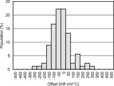
| Gain = 1, 90 units from three production lots |
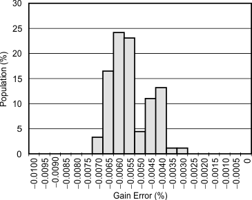
| Gain = 1, 90 units from three production lots |
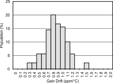
| Gain = 1, 90 units from three production lots |
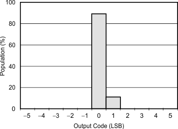
| Gain = 1, data rate = 2.5 SPS, buffer = off, 256 readings |
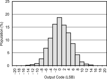
| Gain = 1, data rate = 1 kSPS, buffer = off, 4096 readings |
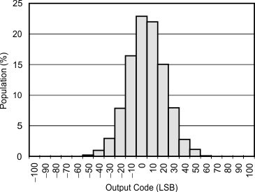
| Gain = 1, data rate = 30 kSPS, buffer = off, 4096 readings |

| Gain = 1 |
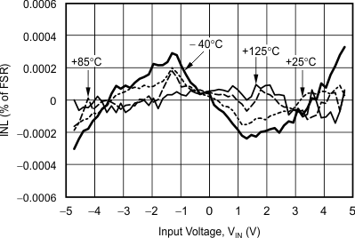
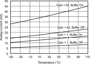
| Gain = 1 |
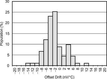
| Gain = 64, 90 units from three production lots |
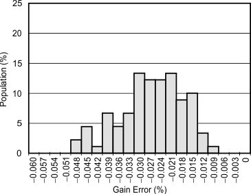
| Gain = 64, 90 units from three production lots |
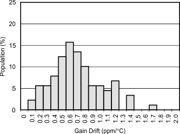
| Gain = 64, 90 units from three production lots |
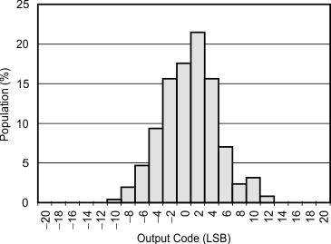
| Gain = 64, data rate = 2.5 SPS, buffer = off, 256 readings |
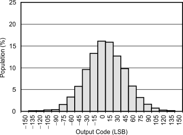
| Gain = 64, data rate = 1 kSPS, buffer = off, 4096 readings |

| Gain = 64, data rate = 30 kSPS, buffer = off, 4096 readings |
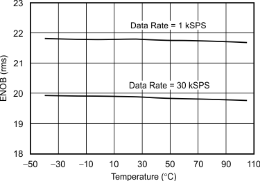
| Gain = 1 |

