ZHCSJC0 January 2019 ADS1260-Q1 , ADS1261-Q1
ADVANCE INFORMATION for pre-production products; subject to change without notice.
- 1 特性
- 2 应用
- 3 说明
- 4 修订历史记录
- 5 Device Comparison Table
- 6 Pin Configuration and Functions
- 7 Specifications
- 8 Parameter Measurement Information
-
9 Detailed Description
- 9.1 Overview
- 9.2 Functional Block Diagram
- 9.3 Feature Description
- 9.4
Device Functional Modes
- 9.4.1 Conversion Control
- 9.4.2 Chop Mode
- 9.4.3 AC-Excitation Mode
- 9.4.4 ADC Clock Mode
- 9.4.5 Power-Down Mode
- 9.4.6 Reset
- 9.4.7 Calibration
- 9.5 Programming
- 9.6
Register Map
- 9.6.1 Device Identification (ID) Register (address = 00h) [reset = xxh]
- 9.6.2 Device Status (STATUS) Register (address = 01h) [reset = 01h]
- 9.6.3 Mode 0 (MODE0) Register (address = 02h) [reset = 24h]
- 9.6.4 Mode 1 (MODE1) Register (address = 03h) [reset = 01h]
- 9.6.5 Mode 2 (MODE2) Register (address = 04h) [reset = 00h]
- 9.6.6 Mode 3 (MODE3) Register (address = 05h) [reset = 00h]
- 9.6.7 Reference Configuration (REF) Register (address = 06h) [reset = 05h]
- 9.6.8 Offset Calibration (OFCALx) Registers (address = 07h, 08h, 09h) [reset = 00h, 00h, 00h]
- 9.6.9 Full-Scale Calibration (FSCALx) Registers (address = 0Ah, 0Bh, 0Ch) [reset = 00h, 00h, 40h]
- 9.6.10 IDAC Multiplexer (IMUX) Register (address = 0Dh) [reset = FFh]
- 9.6.11 IDAC Magnitude (IMAG) Register (address = 0Eh) [reset = 00h]
- 9.6.12 Reserved (RESERVED) Register (address = 0Fh) [reset = 00h]
- 9.6.13 PGA Configuration (PGA) Register (address = 10h) [reset = 00h]
- 9.6.14 Input Multiplexer (INPMUX) Register (address = 11h) [reset = FFh]
- 9.6.15 Input Bias (INPBIAS) Register (address = 12h) [reset = 00h]
- 10Application and Implementation
- 11Power Supply Recommendations
- 12Layout
- 13器件和文档支持
- 14机械、封装和可订购信息
12.2 Layout Example
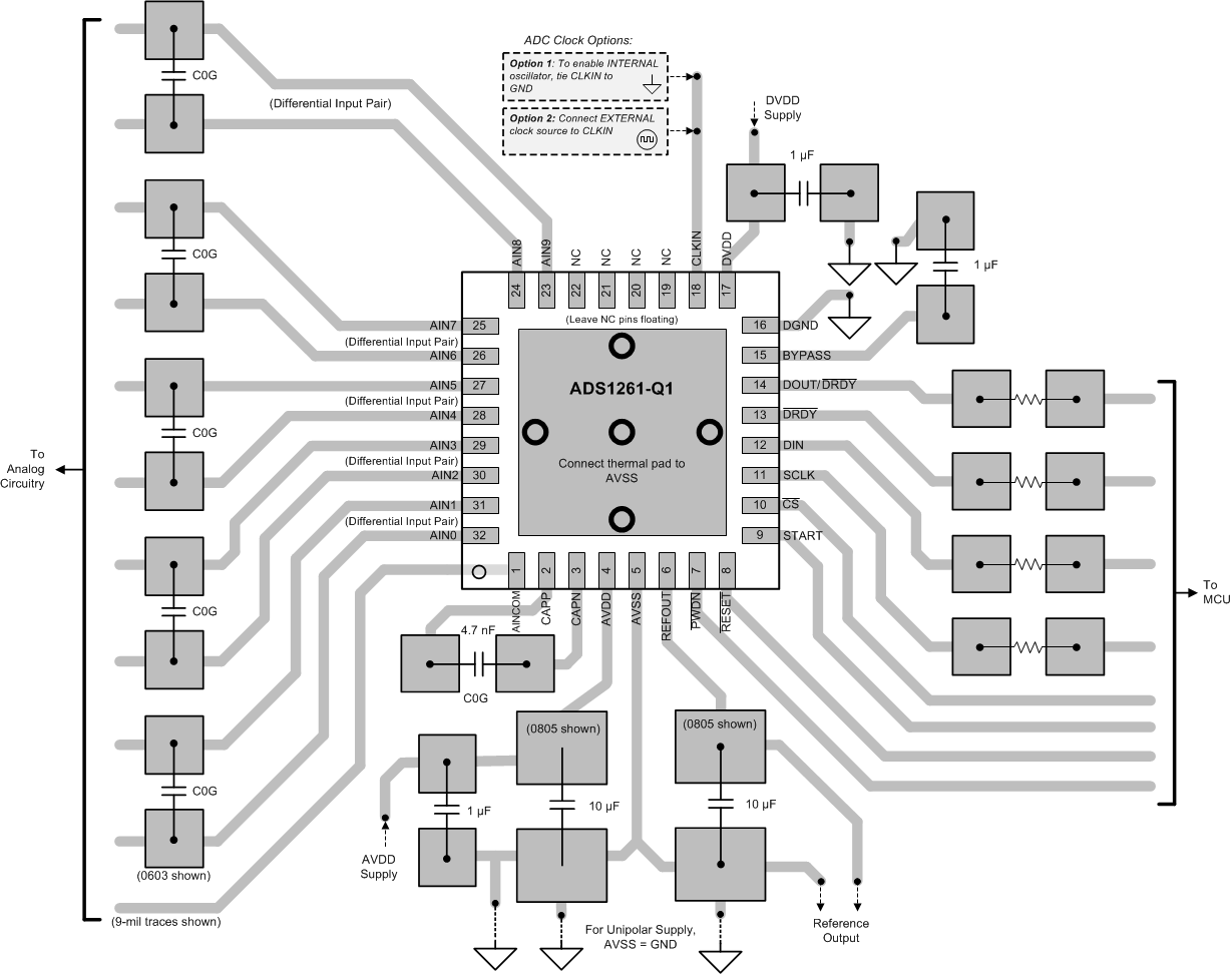
Figure 64 is an example layout of the ADS1261-Q1, requiring a minimum of three PCB layers. The example circuit is shown with single supply operation (AVSS = DGND). In this example, the inner layer is dedicated to the ground plane and the outer layers are used for signal and power traces. If a four-layer PCB is used, dedicate the additional inner layer as the power plane. In this example, the ADC is oriented in such a way to minimize crossover of the analog and digital signal traces.
 Figure 64. ADS1261-Q1 Layout Example