ZHCSIS6B September 2018 – December 2018 ADS1278-SP
PRODUCTION DATA.
- 1 特性
- 2 应用
- 3 说明
- 4 修订历史记录
- 5 说明 (续)
- 6 Pin Configuration and Functions
- 7 Specifications
-
8 Detailed Description
- 8.1 Overview
- 8.2 Functional Block Diagram
- 8.3
Feature Description
- 8.3.1 Sampling Aperture Matching
- 8.3.2 Frequency Response
- 8.3.3 Phase Response
- 8.3.4 Settling Time
- 8.3.5 Data Format
- 8.3.6 Analog Inputs (AINP, AINN)
- 8.3.7 Voltage Reference Inputs (VREFP, VREFN)
- 8.3.8 Clock Input (CLK)
- 8.3.9 Mode Selection (MODE)
- 8.3.10 Synchronization (SYNC)
- 8.3.11 Power-Down (PWDN)
- 8.3.12 Format[2:0]
- 8.3.13 Serial Interface Protocols
- 8.3.14 SPI Serial Interface
- 8.3.15 Frame-Sync Serial Interface
- 8.3.16 DOUT Modes
- 8.3.17 Daisy-Chaining
- 8.3.18 Modulator Output
- 8.3.19 Pin Test Using Test[1:0] Inputs
- 8.3.20 VCOM Output
- 8.4 Device Functional Modes
- 9 Application and Implementation
- 10Power Supply Recommendations
- 11Layout
- 12器件和文档支持
- 13机械、封装和可订购信息
8.3.11 Power-Down (PWDN)
The channels of the ADS1278-SP can be independently powered down by use of the PWDN inputs. To enter the power-down mode, hold the respective PWDN pin low for at least two CLK cycles. To exit power-down, return the corresponding PWDN pin high. Note that when all channels are powered down, the ADS1278-SP enters a microwatt (μW) power state where all internal biasing is disabled. In this state, the TEST[1:0] input pins must be driven; all other input pins can float. The ADS1278-SP outputs remain driven.
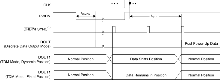
As shown in Figure 71 and Table 10, a maximum of 130 conversion cycles must elapse for SPI interface, and 129 conversion cycles must elapse for Frame-Sync, before reading data after exiting power-down. Data from channels already running are not affected. The user software can perform the required delay time in any of the following ways:
- Count the number of data conversions after taking the PWDN pin high.
- Delay 129/fDATA or 130/fDATA after taking the PWDN pins high, then read data.
- Detect for non-zero data in the powered-up channel.
After powering up one or more channels, the channels are synchronized to each other. It is not necessary to use the SYNC pin to synchronize them.
When a channel is powered down in TDM data format, the data for that channel are either forced to zero (fixed-position TDM data mode) or replaced by shifting the data from the next channel into the vacated data position (dynamic-position TDM data mode).
In Discrete data format, the data are always forced to zero. When powering-up a channel in dynamic-position TDM data format mode, the channel data remain packed until the data are ready, at which time the data frame is expanded to include the just-powered channel data. See the Data Format section for details.
 Figure 71. Power-Down Timing
 Table 10. Power-Down Timing
| SYMBOL | DESCRIPTION | MIN | TYP | MAX | UNITS |
|---|---|---|---|---|---|
| tPWDN | PWDN pulse width to enter Power-Down mode | 2 | CLK periods | ||
| tNDR | Time for new data ready (SPI) | 129 | 130 | Conversions (1/fDATA) | |
| tNDR | Time for new data ready (Frame-Sync) | 128 | 129 | Conversions (1/fDATA) |