ZHCSIS6B September 2018 – December 2018 ADS1278-SP
PRODUCTION DATA.
- 1 特性
- 2 应用
- 3 说明
- 4 修订历史记录
- 5 说明 (续)
- 6 Pin Configuration and Functions
- 7 Specifications
-
8 Detailed Description
- 8.1 Overview
- 8.2 Functional Block Diagram
- 8.3
Feature Description
- 8.3.1 Sampling Aperture Matching
- 8.3.2 Frequency Response
- 8.3.3 Phase Response
- 8.3.4 Settling Time
- 8.3.5 Data Format
- 8.3.6 Analog Inputs (AINP, AINN)
- 8.3.7 Voltage Reference Inputs (VREFP, VREFN)
- 8.3.8 Clock Input (CLK)
- 8.3.9 Mode Selection (MODE)
- 8.3.10 Synchronization (SYNC)
- 8.3.11 Power-Down (PWDN)
- 8.3.12 Format[2:0]
- 8.3.13 Serial Interface Protocols
- 8.3.14 SPI Serial Interface
- 8.3.15 Frame-Sync Serial Interface
- 8.3.16 DOUT Modes
- 8.3.17 Daisy-Chaining
- 8.3.18 Modulator Output
- 8.3.19 Pin Test Using Test[1:0] Inputs
- 8.3.20 VCOM Output
- 8.4 Device Functional Modes
- 9 Application and Implementation
- 10Power Supply Recommendations
- 11Layout
- 12器件和文档支持
- 13机械、封装和可订购信息
8.3.18 Modulator Output
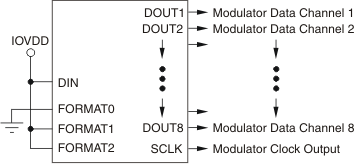
The ADS1278-SP incorporates a 6th-order, single-bit, chopper-stabilized modulator followed by a multi-stage digital filter that yields the conversion results. The data stream output of the modulator is available directly, bypassing the internal digital filter. The digital filter is disabled, reducing the DVDD current, as shown in Table 13. In this mode, an external digital filter implemented in an ASIC, FPGA, or similar device is required. To invoke the modulator output, tie FORMAT[2:0], as shown in Figure 80. DOUT[8:1] then becomes the modulator data stream outputs for each channel and SCLK becomes the modulator clock output. The DRDY/FSYNC pin becomes an unused output and can be ignored. The normal operation of the Frame-Sync and SPI interfaces is disabled, and the functionality of SCLK changes from an input to an output, as shown in Figure 80.
Table 13. Modulator Output Clock Frequencies
| MODE
[1:0] |
CLKDIV | MODULATOR CLOCK OUTPUT (SCLK) | DVDD (mA) |
|---|---|---|---|
| 00 | 1 | fCLK / 4 | 8 |
| 01 | 1 | fCLK / 4 | 7 |
| 10 | 1 | fCLK / 8 | 4 |
| 0 | fCLK / 4 | 4 | |
| 11 | 1 | fCLK / 40 | 1 |
| 0 | fCLK / 8 | 1 |
 Figure 80. Modulator Output
 In modulator output mode, the frequency of the modulator clock output (SCLK) depends on the mode selection of the ADS1278-SP. Table 13 lists the modulator clock output frequency and DVDD current versus device mode.
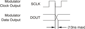
Figure 81 shows the timing relationship of the modulator clock and data outputs.
The data output is a modulated 1s density data stream. When VIN = +VREF, the 1s density is approximately 80% and when VIN = –VREF, the 1s density is approximately 20%.
 Figure 81. Modulator Output Timing