ZHCSF11B April 2016 – September 2016 ADS127L01
PRODUCTION DATA.
- 1 特性
- 2 应用
- 3 说明
- 4 修订历史记录
- 5 Pin Configuration and Functions
-
6 Specifications
- 6.1 Absolute Maximum Ratings
- 6.2 ESD Ratings
- 6.3 Recommended Operating Conditions
- 6.4 Thermal Information
- 6.5 Electrical Characteristics
- 6.6 Timing Requirements: Serial Interface
- 6.7 Switching Characteristics: Serial Interface Mode
- 6.8 Timing Requirements: Frame-Sync Master Mode
- 6.9 Switching Characteristics: Frame-Sync Master Mode
- 6.10 Timing Requirements: Frame-Sync Slave Mode
- 6.11 Switching Characteristics: Frame-Sync Slave Mode
- 6.12 Typical Characteristics
- 7 Parameter Measurement information
-
8 Detailed Description
- 8.1 Overview
- 8.2 Functional Block Diagram
- 8.3 Feature Description
- 8.4 Device Functional Modes
- 8.5
Programming
- 8.5.1 Serial Peripheral Interface (SPI) Programming
- 8.5.2
Frame-Sync Programming
- 8.5.2.1
Frame-Sync Master Mode
- 8.5.2.1.1 Chip Select (CS) in Frame-Sync Master Mode
- 8.5.2.1.2 Serial Clock (SCLK) in Frame-Sync Master Mode
- 8.5.2.1.3 Frame-Sync (DRDY/FSYNC) in Frame-Sync Master Mode
- 8.5.2.1.4 Data Input (DIN) in Frame-Sync Master Mode
- 8.5.2.1.5 Data Output (DOUT) in Frame-Sync Master Mode
- 8.5.2.1.6 Daisy-Chain Input (DAISYIN) in Frame-Sync Master Mode
- 8.5.2.2
Frame-Sync Slave Mode
- 8.5.2.2.1 Chip Select (CS) in Frame-Sync Slave Mode
- 8.5.2.2.2 Serial Clock (SCLK) in Frame-Sync Slave Mode
- 8.5.2.2.3 Frame-Sync (DRDY/FSYNC) in Frame-Sync Slave Mode
- 8.5.2.2.4 Data Input (DIN) in Frame-Sync Slave Mode
- 8.5.2.2.5 Data Output (DOUT) in Frame-Sync Slave Mode
- 8.5.2.2.6 Daisy-Chain Input (DAISYIN) in Frame-Sync Slave Mode
- 8.5.2.1
Frame-Sync Master Mode
- 8.5.3 Data Format
- 8.5.4 Status Word
- 8.5.5 Cyclic Redundancy Check (CRC)
- 8.6
Register Maps
- 8.6.1 ID: ID Control Register (address = 00h) [reset = x3h]
- 8.6.2 CONFIG: ADC Configuration Register (address = 01h) [reset = 00h]
- 8.6.3 OFC0: System Offset Calibration Register 0 (address = 02h) [reset = 00h]
- 8.6.4 OFC1: System Offset Calibration Register 1 (address = 03h) [reset = 00h]
- 8.6.5 OFC2: System Offset Calibration Register 2 (address = 04h) [reset = 00h]
- 8.6.6 FSC0: System Gain Calibration Register 0 (address = 05h) [reset = 00h]
- 8.6.7 FSC1: System Gain Calibration Register 1 (address = 06h) [reset = 80h]
- 8.6.8 MODE: Mode Settings (address = 07h) [reset = xxh]
- 9 Application and Implementation
- 10Power Supply Recommendations
- 11Layout
- 12器件和文档支持
- 13机械、封装和可订购信息
9 Application and Implementation
NOTE
Information in the following applications sections is not part of the TI component specification, and TI does not warrant its accuracy or completeness. TI’s customers are responsible for determining suitability of components for their purposes. Customers should validate and test their design implementation to confirm system functionality.
9.1 Application Information
9.1.1 Unused Inputs and Outputs
Do not float unused digital inputs because excessive power-supply leakage current might result.
The DIN and CS pins are only used in SPI interface mode. Tie DIN (pin 21) and CS (pin 23) directly to DGND when in frame-sync master mode or frame-sync slave mode.
If not daisy-chaining devices, tie DAISYIN directly to DGND.
In SPI interface mode, leave the unused DRDY/FSYNC pin floating, or tie the unused pin to DVDD through high impedance resistors.
9.1.2 Multiple Device Configuration
The ADS127L01 provides configuration flexibility when multiple devices are connected in a system:
- SPI interface mode supports two methods to synchronize multiple devices: cascaded or daisy-chain.
- Frame-sync slave interface mode also supports the same two methods to synchronize multiple devices: cascaded or daisy-chain.
- Frame-sync master interface mode only supports the cascaded method to synchronize multiple devices. Daisy-chain configuration is not available in frame-sync master mode.
9.1.2.1 Cascaded Configuration
Two or more ADS127L01 devices can be cascaded together when using either SPI interface mode or Frame-Sync interface mode. Cascading devices allows multiple devices to share the same interface bus and reduces pin connections to the host processor.
9.1.2.1.1 SPI interface Mode
In SPI interface mode, CLK, SCLK, DIN, and DOUT from each device are shared with independent CS signals. Monitor the DRDY signal from only one device. Leave the remaining DRDY pins floating. Figure 103 shows the required connections for cascading multiple devices in SPI interface mode.
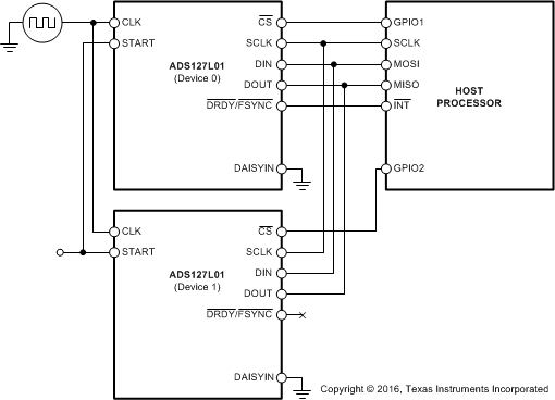 Figure 103. Cascaded Devices in SPI Interface Mode
The host processor must use a separate GPIO to control the CS pins on each ADS127L01 device. When CS is driven to a logic 1, the DOUT of that device is high-impedance. This structure allows another device to take control of the DOUT bus. The SCLK frequency must be high enough to read all of the data from each device before the next DRDY pulse arrives. Alternatively, tie the DOUT pin from each device to a separate pin on the host processor to collect data from multiple devices in parallel.
Equation 9 calculates the maximum number of devices that can share the same bus in a cascaded configuration in terms of data rate, SCLK frequency, and total number of bits per device.
where
- n = 24 or 32 bits
9.1.2.1.2 Frame-Sync interface Mode
In frame-sync interface mode, the CS pin is unused and must be tied to DGND. CLK, SCLK, DIN, and FSYNC from each device are shared with independent DOUT signals. Connect the DOUT pin from each device to a separate input pin on the host processor to read the data from multiple devices in parallel. Figure 104 shows the required connections for cascading multiple devices in frame-sync interface mode.
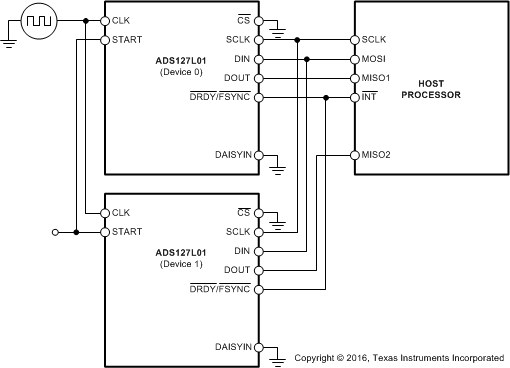 Figure 104. Cascaded Devices in Frame-Sync Mode
Only one device can be configured in frame-sync master mode; remaining devices must be configured in frame-sync slave mode. Otherwise, configure all devices in frame-sync slave mode.
Equation 10 calculates the maximum number of devices that can be daisy-chained for SPI and frame-sync slave mode in terms of data rate, SCLK frequency, and total number of bits to read from each device.
where
- n = 24 or 32 bits
9.1.2.2 Daisy-Chain Configuration
Two or more ADS127L01 devices can be daisy-chained together in either SPI interface mode or frame-sync slave mode. Frame-sync master mode does not support daisy-chain configurations. For both SPI and frame-sync slave mode, connect the DOUT pin of the first device in the chain to an input pin on the host processor. Connect the DOUT pin of the remaining devices to the DAISYIN pin of the next device. Connect the DAISYIN pin on the last device to DGND.
Equation 11 calculates the maximum number of devices that can share the same bus in a cascaded configuration in terms of data rate, SCLK frequency, and total number of bits per device.
where
- n = 32 bits
9.1.2.2.1 Daisy-Chain Operation Using SPI interface Mode
In SPI interface mode, CLK, SCLK, DIN and CS are shared. Monitor only the DRDY signal from one device. Leave the remaining DRDY pins floating. The SCLK frequency must be high enough to read all the data from each device before the next DRDY pulse arrives. Figure 105 shows the required connections for daisy-chaining multiple devices in SPI interface mode.
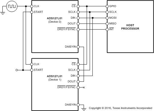 Figure 105. Daisy-Chained Devices in SPI Mode
All data from Device 0 is shifted into Device 1 on the DAISYIN pin. The MSB from the Device 0 data immediately follows the LSB from Device 1 on the DOUT pin of Device 0. Figure 106 illustrates the timing relationship for daisy-chaining devices in SPI interface mode.
 Figure 106. Daisy-Chain Timing in SPI interface Mode
9.1.2.2.2 Daisy-Chain Operation Using Frame-Sync interface Mode
In frame-sync slave mode, CLK, SCLK, DIN and FSYNC are shared. The CS pin is unused and must be tied to DGND. The SCLK frequency must be high enough to read all the data from each device before the next frame begins. Figure 107 shows the required connections for daisy-chaining multiple devices in frame-sync slave mode.
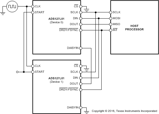 Figure 107. Daisy-Chained Devices in Frame-Sync Slave Mode
All data from Device 1 are shifted into Device 0 on the DAISYIN pin. The MSB from the Device 1 data immediately follows the LSB from Device 0 on the DOUT pin of Device 1. Figure 108 illustrates the timing relationship for daisy-chaining devices in frame-sync slave mode.
 Figure 108. Daisy-Chain Timing in Frame-Sync Slave Mode
9.1.2.3 Synchronizing Devices
Use the START pin or the RESET/PWDN pin to synchronize multiple devices. The START pin does not reset the device registers to the default settings. The RESET/PWDN pin resets the device to the factory default settings, and resets the interface when in frame-sync master mode. The delay from the START signal high to the first data ready is fixed for a given data rate (see the Start Pin (START) section for more details on the delay times).
An alternate way to synchronize multiple devices is using the RESET/PWDN pin. The RESET/PWDN pin resets the digital interface in addition to the digital filters and registers, making it the recommended synchronization method for frame-sync master mode. The delay from the RESET/PWDN pin high to the first data ready is fixed for a given data rate (see the Reset and Power-Down Pin (RESET/PWDN) section for more details on the delay times). The RESET/PWDN pin is also used to synchronize multiple devices in SPI interface mode or frame-sync slave mode.
When synchronizing multiple devices, the master clock, fclk, must be shared from the same signal source.
9.1.3 ADC Input Driver
The input driver circuit for a high-precision delta-sigma ADC consists of two parts: a driving amplifier and a low-pass, antialiasing filter. The amplifier is used to condition the input signal voltage and provide a low output-impedance buffer between the signal source and the switched-capacitor inputs of the ADC. The low-pass antialiasing filter, comprised of series resistors and a differential capacitor, helps to attenuate the voltage transients created by the ADC switched-capacitor input stage, and also serves to band-limit the wideband noise contributed by the front-end circuit. Careful design of the input driver circuit is critical to take advantage of the linearity and noise performance of the ADS127L01.
9.1.3.1 Antialiasing Filter
Signal aliasing in data-acquisition systems occurs when continuous-time signals are discretely sampled at a constant rate. To properly represent an analog signal in the digital domain, the system must sample the input at a sampling rate greater than twice the maximum frequency content, known as the Nyquist rate. Frequencies that are greater than one-half the sampling rate are not represented properly in the digital domain and appear as aliases of the original input instead.
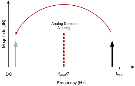
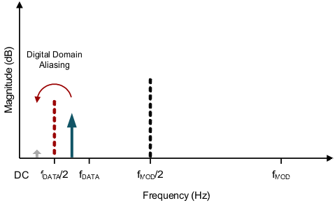
Delta-sigma ADCs exhibit two Nyquist frequencies, as shown in Figure 109. The first Nyquist frequency occurs in the analog domain at one-half the modulator sampling rate (fMOD / 2). The second Nyquist frequency occurs in the digital domain at one-half the decimated output data rate (fDATA / 2). Frequency content repeats at multiples of fMOD and fDATA. Both Nyquist frequencies allow for out-of-band signals to alias into the ADC pass band, including noise from the front-end driver circuit. This aliasing increases the in-band noise level of the system and degrades overall performance if not adequately filtered.
 Figure 109. Delta-Sigma ADC Internal Signal Chain
Figure 110 and Figure 111 illustrate the two aliasing domains in delta-sigma ADCs. Figure 110 shows a higher-frequency, out-of-band signal aliasing around the modulator Nyquist frequency (fMOD / 2) into the pass band. Figure 111 shows a lower-frequency, out-of-band signal aliasing around the data rate Nyquist frequency (fDATA / 2) into the pass band after being attenuated by the digital filter.
To prevent signals from aliasing, use a low-pass antialiasing filter to attenuate the out-of-band signals. The simplest antialiasing filter is a discrete first-order, low-pass, RC filter. To achieve a higher level of attenuation at the Nyquist frequency requires a higher-order filter response, usually before the last amplifier stage.
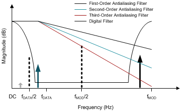
The digital filter in delta-sigma ADCs reduces the attenuation requirement of the antialiasing filter by providing a high stop-band attenuation between fDATA / 2 and fMOD. At multiples of fMOD, the digital filter response returns to 0 dB and repeats. This portion of the digital filter response is the sensitive frequency band where an antialiasing filter is needed. Figure 112 overlays a digital filter response with first-, second-, and third-order antialiasing filters, attenuating both out-of-band signals.
The antialiasing RC filter also helps to attenuate the voltage transients from the sampling network at the ADC inputs. Figure 113 shows a simplified switch-capacitor circuit at the inputs of an ADC modulator. The sampling network, described in Figure 60, places a transient load on the external drive circuit. The differential capacitor in the RC filter, CDIFF, acts as a charge reservoir and transfers charge to the internal sampling capacitor, CSAMPLE, while S1 is closed. The input driver circuit must restore the charge at the input nodes (AINP and AINN) so that the voltage settles before S1 opens. After S1 opens, S2 closes, discharging the CSAMPLE capacitor. The faster the modulator sampling rate, the less time the input voltage has to settle. An amplifier with a gain-bandwidth product (GBP) that is too low fails to provide adequate settling because of the higher output impedance over frequency, and results in increased distortion.
 Figure 113. Delta-Sigma Modulator Sampling Network
The sampling capacitors of the ADS127L01 have an equivalent capacitance of 8 pF. Scale CDIFF to be at least 100 times larger than CSAMPLE. Connect CDIFF directly across the ADC input pins to help provide adequate charge with each ADC sample. CDIFF must be C0G or NP0 dielectric type because these components have a high-Q, low-temperature coefficient, and stable electrical characteristics to withstand varying voltages and frequencies. Common-mode capacitors, CCM, can also be added at each input to ground to attenuate common-mode noise and sampling glitches. Size the common-mode capacitors to be one order of magnitude smaller than CDIFF in order to maintain system common-mode rejection (CMR).
Figure 114 shows an example of the voltage transient created by the ADC sampling event at the inputs of an unbuffered delta-sigma ADC. The larger transients mark the moment when S1 closes to connect CSAMPLE to the external front-end circuitry. The smaller transient occurs when the S1 switch opens passing the charge through the modulator. The sequence repeats at 1 / fMOD. The data were recorded using a passive 10x probe on the AINP pin only. The same transient is observed on AINN as well. The differential transient voltage is more than an order of magnitude smaller.
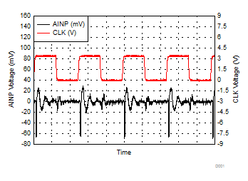 Figure 114. ADC Input During Sampling
When S1 opens, the input signal is sampled and converted by the modulator. Increasing CDIFF provides a larger charge reservoir to the ADC, and reduces the initial voltage droop. For ADCs with a faster sampling frequency, there is less time for this voltage transient to fully settle before the next sample. The ADC input relies on a driver amplifier with sufficient bandwidth and low output impedance at high frequencies to provide recovery charge and fully settle the voltage transient before S1 opens.
9.1.3.2 Input Driver Selection
Selection criteria for the input amplifiers are highly dependent on the input signal type, as well as the performance goals of the data-acquisition system. Consider the following amplifier specifications when selecting the appropriate driver amplifier for the application:
- Noise. The output noise density of the front-end amplifiers must be kept as low as possible to prevent any degradation in system SNR performance. The total noise from the input stage is determined by the –3-dB bandwidth of the ADS127L01 digital filter. Make sure that the total output noise is less than 20% of the input-referred noise of the ADC, as explained in Equation 12:
- eo_RMS = Broadband output noise of the input driver stage in nV/√Hz
- f-3dB = –3-dB bandwidth of the ADS127L01 digital filter in Hz
- Distortion. Keep the distortion from the front-end drivers as low as possible, especially in the presence of a switching load. Harmonics produced by the amplifier are also compounded by harmonics produced by the ADC. Minimize the amplifier distortion by using the widest allowable supply voltage and highest output load resistance for the application. Select an amplifier with high open-loop gain and at least –10 dB better distortion than the ADC distortion in order to prevent any degradation to system THD performance, as explained by Equation 13.
- THDAMP = Total harmonic distortion from input driver
- THDADC = Total harmonic distortion specification of the ADC
- Small-signal bandwidth. Select the small-signal bandwidth of the input amplifiers to be as high as possible, after meeting the power budget of the system. Higher bandwidth reduces the closed-loop output impedance of the amplifier, thus allowing the amplifier to more easily drive a larger capacitive load with a smaller series resistor. For a given low-pass filter cutoff, keep the series resistor as small as possible and increase the differential capacitor to minimize gain error and distortion (see the Antialiasing Filter section). Higher bandwidth also minimizes harmonic distortion caused by faster settling of the input transients from the ADC sampling. The required amplifier bandwidth depends on the size of the sampling capacitor, the sampling frequency, and the size of the external differential capacitor. TINA-TI simulations help model the small-signal settling behavior and the stability of the input driver circuit for a given load.

where

where
The THS45xx family of fully-differential amplifiers offers the low noise and distortion specifications needed in high-performance data-acquisition systems. Table 30 shows the power versus performance tradeoff offered between the THS4531A, THS4551, and the highest performing THS4541.
Table 30. Input Driver Selection
| DRIVER | GAIN BANDWIDTH PRODUCT (MHz) | NOISE DENSITY (nV/√Hz) | QUIESCENT CURRENT Iq (mA) | NOMINAL RF AND RG (Ω) |
|---|---|---|---|---|
| THS4531A | 36 | 10 | 0.23 | 2 k |
| THS4551 | 135 | 3.4 | 1.31 | 1.2 k |
| THS4541 | 850 | 2.2 | 9.7 | 402 |
Figure 115 and Figure 116 compare the distortion and noise performance of the THS4531A, THS4541, and THS4551 as they drive the inputs of the ADS127L01. Each input driver circuit was configured for a gain of one using the nominal feedback resistor values in Table 30. An AP2700 function generator provided a full-scale, sine wave input at frequencies of 2 kHz and below, such that at least five harmonics were present in the fast Fourier transform (FFT) calculated from 8,192 samples. An Agilent 33522A provided the clock input for the ADS127L01 (CLK) to set the modulator clock frequency between 100 kHz and 16.384 MHz.
To quantify the distortion performance of each input driver circuit, the spurious-free dynamic range (SFDR) is calculated at each modulator clock frequency. A third-order polynomial, best-fit curve is applied to the raw data to show the overall trend for each amplifier.
Figure 115 illustrates that at slower modulator clock frequencies, a lower power amplifier with less bandwidth can be used to achieve similar SFDR performance as higher power amplifiers with more bandwidth. However, faster modulator clock frequencies require the use of a wide-bandwidth amplifier to get the best performance out of the ADC.
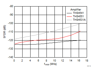 Figure 115. SFDR vs fMOD
In contrast to SFDR, the signal-to-noise ratio (SNR) of a data-acquisition signal chain is more dependent on the input amplifier noise density, as well as the ADC output data rate. Figure 116 displays the SNR performance of the ADS127L01 measured while driving the inputs with the THS4531A, THS4541, and THS4551. The digital filter in the ADS127L01 is configured to use the Wideband 2 transition band and an OSR of 256 throughout the SNR measurements. An AP2700 provided a small-signal 1 kHz input sine wave of 100 mVpp. An Agilent 33522A provided the clock input (CLK) for the ADS127L01 to set the modulator clock frequency between 100 kHz and 16.384 MHz. The measured SNR is normalized to full-scale.
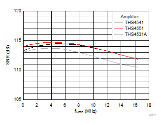 Figure 116. SNR vs fMOD
The SNR performance is expected to remain relatively constant for all three amplifiers across modulator frequencies. However, the improvement in SNR at slower modulator frequencies is because of the reduced bandwidth of the digital filter as it scales down with modulator clock, limiting the input source broadband noise. At higher frequencies, noise from the input source dominates as the digital-filter bandwidth increases. The difference in amplifier noise density, listed in Table 30, has the largest effect on the system noise performance.
9.1.3.3 Amplifier Stability
Driving a capacitive load can degrade the phase margin of the input amplifier, and can make the amplifier unstable. To prevent the amplifier from becoming unstable, a series isolation resistor (RFLT) is used at the amplifier output, as shown in Figure 113. A higher resistance value increases phase margin and makes the amplifier more stable, but also increases distortion caused by the interaction with the nonlinear input impedance of the ADC modulator. Distortion increases with source output impedance, input-signal frequency, and input-signal amplitude.
The selection of RFLT requires a balance between distortion and the stability of the input driver design. The use of 1% components is allowed because the CDIFF mitigates the degradation of CMR caused by input imbalances.
The input amplifier must be selected with a bandwidth higher than the cutoff frequency, fC, of the antialiasing filter at the ADC inputs. Use a TINA-TI simulation to confirm that the amplifier has more than 30° of phase margin when driving the selected filter to verify stability. Simulation is critical because some amplifiers require more bandwidth than others to drive the same filter. If the input amplifier circuit has less than 20° of phase margin, consider adding a capacitor at the amplifier inputs to increase phase margin.
9.1.4 Modulator Saturation
The ADS127L01 features a third-order modulator and a 5-bit quantizer in order to achieve excellent SNR performance, resolution, and linearity. However, as with all high-order, delta-sigma modulators, certain input conditions may saturate the modulator and increase the quantization noise. These conditions include input signals that are less than full-scale and contain frequency content that falls within the stop band of the digital filter. Most notably, a saturated modulator increases the ADC in-band noise floor and degrades SNR performance.
To prevent the ADS127L01 from reaching a saturated condition, use an antialiasing filter at the inputs to attenuate out-of-band signals. Table 31 shows the differential input amplitude limits at frequencies from 100 kHz to 15 MHz for discrete modulator rates in order to prevent saturation. In general, a multiple-order, low-pass response with a –3-dB cutoff placed one decade beyond the pass band is sufficient for most applications.
Table 31. Differential Input Amplitude Limits (dBFS)
| fIN (MHz) | fMOD | |||
|---|---|---|---|---|
| 4.096 MHz | 8.192 MHz | 12 MHz | 16.384 MHz | |
| 0.1 | 0 | — | — | — |
| 0.2 | 0 | 0 | — | — |
| 1 | –3 | –2 | –2 | –2 |
| 2 | –7 | –6.5 | –3 | –2.5 |
| 8 | –18 | –18 | –18 | –18 |
| 10 | –19 | –19 | –19 | –19 |
| 15 | –20 | –20 | –20 | –20 |
9.1.5 ADC Reference Driver
Design the reference driver to provide a precision, low-drift reference voltage to the ADC for best performance. Similar to the input of the ADC, a switched-capacitor circuit samples the reference voltage between REFP and REFN. The switched capacitor imposes a transient load on the external reference driver circuit at the modulator frequency. A reference buffer is required to restore the charge across the differential capacitor at the reference input pins so that the voltage settles before the next acquisition. The integrated broadband reference noise must remain significantly less than the ADC integrated noise to minimize SNR degradation. Choose a reference driver with relatively low noise density. Reference noise can be heavily filtered with a low-pass filter.
Below are two options for driving the reference input of the ADS127L01. Option 1 presents a single-chip solution with an integrated buffer. Option 2 presents a multichip solution with a precision reference and an external buffer.
9.1.5.1 Single Chip Solution: REF6xxx
The REF6xxx is a family of very high-precision, low-noise, and low-drift voltage references. This single-chip solution has an integrated high-bandwidth buffer that presents a low output impedance to the ADC reference input. The REF6025 outputs a fixed 2.5-V output voltage; however, other devices from the same family are available to offer various output voltages and temperature drift specifications
The ADS127L01 has the ability to maintain a high level of performance at relatively low levels of power consumption. The REF6025 only adds 750 μA of typical quiescent current to the system power budget, while still showcasing the performance of the ADS127L01 when sampling at full-speed, making it a great fit for low-power applications with limited board space.
Figure 117 shows typical connections for the REF6025 as a reference driver circuit to the ADS127L01. The output of the REF6025 uses a Kelvin connection to correct for the voltage drop between the voltage output pins and the pads of the output capacitor. A small series resistance is required to keep the reference output stable. See the REF60xx device datasheet (SBOS708) for more details on the required connections and component values.
 Figure 117. REF6025 Connection to ADS127L01
9.1.5.2 Multichip Solution: REF50xx + OPA320
The REF50xx is another family of low-noise, low-drift, high-precision voltage references. The REF5025 outputs a fixed 2.5-V output voltage; however, other devices from the same family are available to offer various output voltages. Buffer the output of the REF5025 with a low-noise, wide bandwidth amplifier such as the OPA320 to achieve the best performance with the ADS127L01.
The OPA320 is a precision, low-voltage CMOS operational amplifier optimized for low noise and wide bandwidth with a typical quiescent current of 1.5 mA. From 0.1 Hz to 10 Hz, the OPA320 features an output noise of 2.8 µVPP. With a unity gain-bandwidth product of 20 MHz, the OPA320 is able to drive the ADS127L01 reference inputs while sampling at full-speed without degrading linear performance of the system.
Figure 118 shows an example reference circuit using the REF5025 and the OPA320. The output of the REF5025 is low-pass filtered to less than 2 Hz before the input of the OPA320. The OPA320 is placed in a noninverting buffer configuration with dual-feedback to compensate for the large capacitive output load and maintain stability. See the respective device data sheets for more details on the required connections and component values.
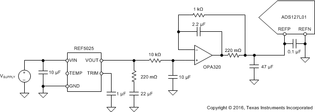 Figure 118. REF5025 + OPA320 Connection to ADS127L01
Table 32 compares the performance characteristics of the two reference driver solutions discussed in this section.
Table 32. Reference Selection
| DEVICE | IQ (μA) | TEMPERATURE DRIFT TYP (μV/°C) | TEMPERATURE DRIFT MAX (μV/°C) | NOISE (μVPP)(1) | TEMPERATURE RANGE (°C) |
|---|---|---|---|---|---|
| REF5025 + OPA320 | 2300 | 8.0 | 22.9 | 9.04 | -40°C to +125°C |
| REF6025 | 750 | 7.5 | 12.5 | 20.53 | -40°C to +125°C |
| REF6125 | 750 | 10.0 | 20 | 20.53 | -40°C to +125°C |
The two reference solutions are capable of driving the ADS127L01 to meet datasheet specifications. While the multichip solution has a larger PCB footprint, the multichip solution offers similar noise performance, and allows more customization than the REF6x25, including the ability to low-pass filter the broadband noise of the REF5025. This multichip solution may provide a lower-cost alternative to the REF6x25 for applications that can tolerate a higher component count and power consumption. The REF6x25 has a smaller PCB footprint, and offers tighter drift specifications at a fraction of the power.
9.1.6 Driving LVDD With an External Supply
A portion of the ADC modulator in the ADS127L01 is powered from a separate low-voltage analog supply (LVDD) to achieve lower overall power consumption. This supply is nominally 1.8 V and can be sourced by either an internal LDO (INTLDO = 0) or an external supply (INTLDO = 1). When the internal LDO supply is used, the LVDD current is sourced from AVDD.
While LDOs are known to be smaller and less noisy than other power supply topologies, LDOs are much less efficient and can consume large amounts of power. An LDO dissipates excess power as heat in order to regulate the output voltage. The higher the dropout voltage is between the supply input and the LDO output, the more power is wasted.
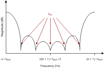
Alternatively, an external switching power supply can drive LVDD. Switching power supplies are much more efficient and consume less power; however, a small switching ripple could appear on the output. The frequency content from this ripple can appear in the ADC output if:
- The switching frequency falls directly in the ADC pass band.
- The switching frequency aliases into the ADC pass band from an out-of-band frequency.
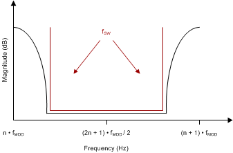
Consider carefully when choosing the switching frequency (fSW) in order to maintain the highest system power-supply rejection (PSR). The LVDD supply pin offers at least 75 dB of PSR at 60 Hz. Choose an out-of-band switching frequency that falls within the stop band of the wideband FIR filter, or within the notches of the low-latency sinc filter, as shown in Figure 119 and Figure 120, respectively. If possible, an ideal design synchronizes the switching supply frequency to a 1/2n ratio of the modulator clock frequency. Any remaining frequency content that is not suppressed by the LVDD PSR will fall into the nulls of the digital filter or fold back to dc.
9.2 Typical Application
Test and measurement applications interface sensor inputs with a precision data-acquisition signal chain. This signal chain must be capable of measuring a wide frequency range with very low noise and minimal harmonic distortion. Figure 121 illustrates the main components of a sensor signal chain, consisting of a conditioning stage at the sensor output, followed by a high-speed, low-noise amplifier driving a wide-bandwidth, delta-sigma ADC.
 Figure 121. Test and Measurement Block Diagram
In data-acquisition systems, signal distortion can come from the amplifier, the settling of the switched-capacitor load transients, and the ADC. Choose both the differential drive amplifier and the ADC such that neither one limits the distortion performance of the signal chain. This section details the design procedure for the fully-differential input stage to an ADC optimized for low noise and minimal harmonic distortion.
9.2.1 Design Requirements
Table 33. Design Requirements
| DESIGN PARAMETER | VALUE |
|---|---|
| Analog supply voltage | 3.0 V |
| Modulator sampling frequency (fMOD) | 16 MHz |
| Filter pass band | DC to 100 kHz (fDATA = 250 kSPS) |
| Antialiasing filter rejection | –100 dB at fMOD |
| Total harmonic distortion (THD) | –110 dB at –0.5-dBFS input signal amplitude |
| Signal-to-noise ratio (SNR) | 70 dB at 100-mV input signal amplitude (104 dB normalized to 2.5-V full-scale) |
| Power consumption | 20 mA (50 mW) ADS127L01, input drive amplifier, reference device + drive amplifier |
9.2.2 Detailed Design Procedure
The ADS127L01 offers a typical THD level of –110 dB for a modulator frequency of 16.384 MHz. Target the distortion from the input driver to be at least 10 dB better than the distortion of the ADC. The THS4551 provides exceptional ac performance with extremely low distortion levels near –120 dB. With a 135-MHz gain-bandwidth product, the THS4551 can drive the switched-capacitor input stage so that the load transients are mostly settled. For higher levels of performance, use a faster amplifier with more bandwidth as long as the increased current consumption fits within the system power budget. At 3.4 nV/√Hz broadband noise density and 1.35 mA of quiescent current, the THS4551 offers an attractive performance versus power tradeoff that is well-suited for these applications.
Single-ended inputs have a varying input common-mode, and can produce larger even harmonics and decrease distortion performance. Use a fully-differential input to the ADC to help suppress even harmonics and provide a fixed common-mode voltage for the input signal.
For this design, the THS4551 is placed in a multiple-feedback (MFB) filter configuration, as shown in Figure 122. Nominal resistance values of 1.2 kΩ are used in the amplifier feedback path to optimize power consumption, while keeping the added broadband noise of the front-end driver circuit less than that of the ADS127L01. An MFB filter produces a second-order, low-pass response.
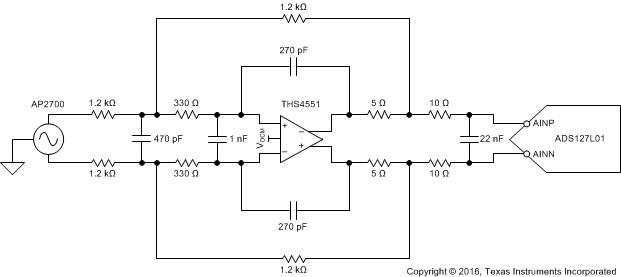 Figure 122. Multiple Feedback ADC Drive Circuit
The discrete low-pass RC filter components (10 Ω and 22 nF) are small enough to increase the antialiasing filter rolloff without adding significant distortion or gain error to the system. Combined with the active MFB filter, the net result is a third-order antialiasing filter. Figure 123 plots the magnitude response of the front-end driver circuit and illustrates how it supplements the Wideband 2 FIR filter in the ADS127L01.
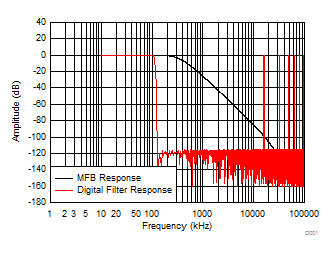
The response of the third-order antialiasing filter remains flat beyond the digital filter pass band. Signals within the bandwidth of interest are left unattenuated by the antialiasing filter. The Wideband 2 filter is used to provide an average stop-band attenuation of –116 dB beginning at fDATA / 2. This transition band prevents signals from aliasing in the digital domain.
At fc = 304 kHz, the antialiasing filter reaches –3 dB, and rolls off sharply at a rate of –60 dB per decade. At 16 MHz, the filter response reaches –100 dB of attenuation, effectively eliminating unwanted frequency content around the modulator rate. The antialiasing filter attenuates the frequency content that alias around the modulator Nyquist frequency (fMOD / 2). The REF6025 circuit proposed in Figure 117 was selected to drive the ADS127L01 reference. This device enables the design to meet the outlined performance goals while remaining within the target power budget.
9.2.3 Application Curves
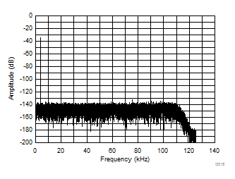
Figure 124 shows a fast Fourier transform (FFT) of the 32,768 samples collected at 250 kSPS (OSR 64). An AP2700 generated a 4-kHz sine wave with a differential amplitude of –0.5 dB below full-scale (±2.36 V). The fundamental input frequency at 4 kHz is the dominate tone in the FFT. The first 15 harmonics are used to calculate the total harmonic distortion (THD) as –114.4 dB. The input amplifier and the antialiasing filter do not degrade the overall distortion performance of the signal chain.
SNR was measured with a small-signal 100 mVPP (–34 dB from full-scale) input sine wave generated by the AP2700. The SNR result is the difference in magnitude between the fundamental frequency and the integrated noise of the ADC output up until fDATA / 2. Figure 125 shows the FFT of the 32,768 samples collected at 256 kSPS (OSR = 64). The result is then normalized to full-scale to yield 106.3 dB.
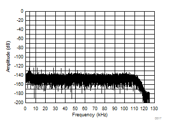
| fIN = 4 kHz, amplitude = –0.5 dBFS, THD = –114.4 dB |
| fIN = 4 kHz, amplitude = 100 mVPP, SNR = 106.3 dB (normalized to FS) |
To verify the effectiveness of an antialiasing filter, input a sine wave at the frequency of interest and measure how much that signal is attenuated at the output. In order to measure the attenuation at fMOD = 16 MHz, input a signal around or at that frequency and measure the alias of the signal that folds into the ADC pass band.
Figure 126 shows the FFT results of the 32,768 samples collected at 64 kSPS (OSR 256) for finer frequency bin resolution. An Agilent 33522A was used to generate a differential -0.5 dBFS sine wave input at 16.004 MHz. Because 16.004 MHz is offset from 16 MHz (fMOD) by 4 kHz, the input signal aliases to 4 kHz. The magnitude of the frequency tone is the attenuation level of the antialiasing filter.
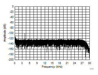
| fMOD = 16 MHz, fIN= 16.004 MHz, amplitude = –0.5 dBFS, OSR = 256 (64 kSPS) |
Table 34 lists the typical current consumption and power dissipation for the ADS127L01, the THS4551, and the REF6025.
Table 34. Power Consumption
| COMPONENT | QUIESCENT CURRENT (mA) | POWER DISSIPATION (mW) |
|---|---|---|
| ADS127L01 (AVDD) | 10.6 | 31.8 |
| ADS127L01 (DVDD) | 4.4 | 7.8 |
| THS4551 | 1.3 | 3.9 |
| REF6025 | 0.8 | 2.3 |
| TOTAL | 17.1 | 45.8 |
9.3 Do's and Don'ts
- Do partition the analog, digital, and power supply circuitry into separate sections on the printed circuit board (PCB).
- Do use a single ground plane for analog and digital grounds.
- Do place the analog components close to the ADC pins using short, direct connections.
- Do keep the SCLK pin free of glitches and noise.
- Do verify that the analog input voltages are within the specified input voltage range under all input conditions.
- Do tie unused digital input pins to DGND to minimize input leakage current.
- Do use an LDO to reduce voltage ripple generated by switch-mode power supplies.
- Do synchronize clock signals and switching supply frequencies to minimize intermodulation artifacts and noise degradation.
- Don't cross analog and digital signals.
- Don't route digital clock traces in the vicinity of the analog inputs or CAP1 and CAP2 analog bias voltages.
- Don't allow the analog and digital power supply voltages to exceed 3.9 V under any condition, including during power-up and power-down.
- Don’t use inductive supply or ground connections.
- Don’t isolate analog ground (AGND) from digital ground (DGND).
Figure 127 illustrates examples of correct and incorrect ADC circuit connections.
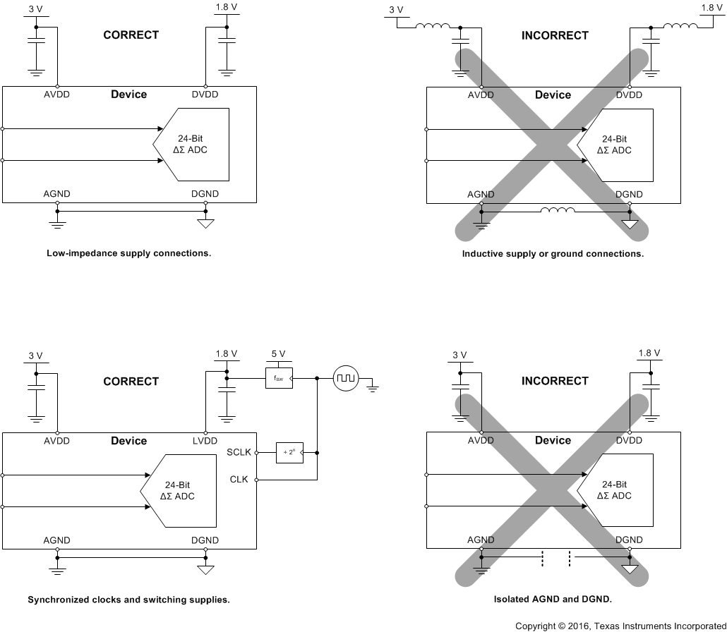 Figure 127. Correct and Incorrect Circuit Connections
9.4 Initialization Setup
Figure 128 illustrates a general procedure to configure the ADS127L01 to collect data.
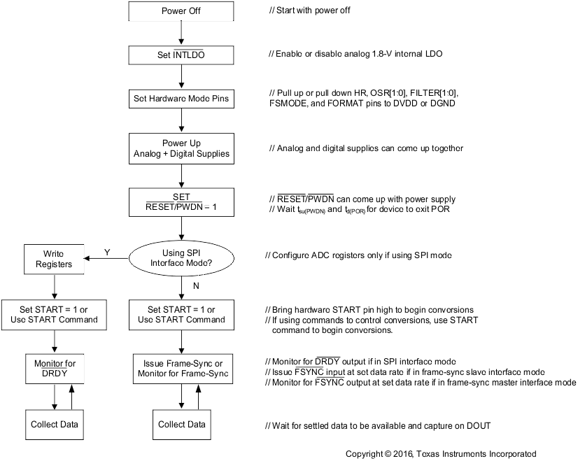 Figure 128. ADS127L01 Configuration Sequence
