ZHCSF11B April 2016 – September 2016 ADS127L01
PRODUCTION DATA.
- 1 特性
- 2 应用
- 3 说明
- 4 修订历史记录
- 5 Pin Configuration and Functions
-
6 Specifications
- 6.1 Absolute Maximum Ratings
- 6.2 ESD Ratings
- 6.3 Recommended Operating Conditions
- 6.4 Thermal Information
- 6.5 Electrical Characteristics
- 6.6 Timing Requirements: Serial Interface
- 6.7 Switching Characteristics: Serial Interface Mode
- 6.8 Timing Requirements: Frame-Sync Master Mode
- 6.9 Switching Characteristics: Frame-Sync Master Mode
- 6.10 Timing Requirements: Frame-Sync Slave Mode
- 6.11 Switching Characteristics: Frame-Sync Slave Mode
- 6.12 Typical Characteristics
- 7 Parameter Measurement information
-
8 Detailed Description
- 8.1 Overview
- 8.2 Functional Block Diagram
- 8.3 Feature Description
- 8.4 Device Functional Modes
- 8.5
Programming
- 8.5.1 Serial Peripheral Interface (SPI) Programming
- 8.5.2
Frame-Sync Programming
- 8.5.2.1
Frame-Sync Master Mode
- 8.5.2.1.1 Chip Select (CS) in Frame-Sync Master Mode
- 8.5.2.1.2 Serial Clock (SCLK) in Frame-Sync Master Mode
- 8.5.2.1.3 Frame-Sync (DRDY/FSYNC) in Frame-Sync Master Mode
- 8.5.2.1.4 Data Input (DIN) in Frame-Sync Master Mode
- 8.5.2.1.5 Data Output (DOUT) in Frame-Sync Master Mode
- 8.5.2.1.6 Daisy-Chain Input (DAISYIN) in Frame-Sync Master Mode
- 8.5.2.2
Frame-Sync Slave Mode
- 8.5.2.2.1 Chip Select (CS) in Frame-Sync Slave Mode
- 8.5.2.2.2 Serial Clock (SCLK) in Frame-Sync Slave Mode
- 8.5.2.2.3 Frame-Sync (DRDY/FSYNC) in Frame-Sync Slave Mode
- 8.5.2.2.4 Data Input (DIN) in Frame-Sync Slave Mode
- 8.5.2.2.5 Data Output (DOUT) in Frame-Sync Slave Mode
- 8.5.2.2.6 Daisy-Chain Input (DAISYIN) in Frame-Sync Slave Mode
- 8.5.2.1
Frame-Sync Master Mode
- 8.5.3 Data Format
- 8.5.4 Status Word
- 8.5.5 Cyclic Redundancy Check (CRC)
- 8.6
Register Maps
- 8.6.1 ID: ID Control Register (address = 00h) [reset = x3h]
- 8.6.2 CONFIG: ADC Configuration Register (address = 01h) [reset = 00h]
- 8.6.3 OFC0: System Offset Calibration Register 0 (address = 02h) [reset = 00h]
- 8.6.4 OFC1: System Offset Calibration Register 1 (address = 03h) [reset = 00h]
- 8.6.5 OFC2: System Offset Calibration Register 2 (address = 04h) [reset = 00h]
- 8.6.6 FSC0: System Gain Calibration Register 0 (address = 05h) [reset = 00h]
- 8.6.7 FSC1: System Gain Calibration Register 1 (address = 06h) [reset = 80h]
- 8.6.8 MODE: Mode Settings (address = 07h) [reset = xxh]
- 9 Application and Implementation
- 10Power Supply Recommendations
- 11Layout
- 12器件和文档支持
- 13机械、封装和可订购信息
8 Detailed Description
8.1 Overview
The ADS127L01 is a 24-bit delta-sigma (ΔΣ) ADC that offers a combination of excellent dc accuracy and ac performance. The flexible digital-filter options make it suitable for both dc and ac applications. The device is hardware programmable, making it easy to configure for a variety of applications without the need to program any registers.
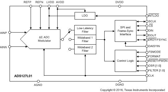
The Functional Block Diagram shows the main internal features of the ADS127L01. The converter is comprised of a third-order, chopper-stabilized, delta-sigma modulator, that measures the differential input signal, VIN = (VAINP – VAINN), against the differential reference, VREF = (VREFP – VREFN). The converter core consists of a differential, switched-capacitor, delta-sigma modulator followed by a selectable digital filter. The digital-filter low-latency path uses a cascaded combination of a fifth-order sinc and a first-order sinc filter, ideal for applications requiring fast response time or systems using a multiplexed input. Two wide-bandwidth paths (Wideband 1 and Wideband 2) are also available, providing outstanding frequency response with very low pass-band ripple, a steep-transition band, and high stop-band attenuation. The ADS127L01 provides two selectable options for transition-band frequency. The Wideband-filter paths are suited for applications that require high-resolution measurements of high-frequency, ac-signal content. To allow tradeoffs among speed, resolution, and power, three operating modes are supported: high-resolution (HR), low-power (LP), and very-low-power (VLP).
In HR mode, SNR = 104.4 dB (VREF = 2.5 V) at a maximum data rate of 512 kSPS. At this data rate, the power dissipation is only 35 mW, and scales with master clock frequency. In LP mode, the maximum data rate is 256 kSPS, while consuming only 19 mW of power. In VLP mode, the maximum data rate is 128 kSPS, while consuming only 9 mW of power.
Configure the ADS127L01 by setting the appropriate hardware I/O pins. Registers are available for gain and offset calibrations. Three interface communication modes are available, providing flexibility for convenient interfacing to microcontrollers, DSPs, or FPGAs. SPI, frame-sync slave, or frame-sync master communication modes are hardware selectable on the device. The ADS127L01 has a daisy-chain output available, and can synchronize externally to another device or system using the START signal. The daisy-chain configuration allows the device to be used conveniently in systems that require multiple channels.
8.2 Functional Block Diagram
8.3 Feature Description
This section discusses the details of the ADS127L01 internal functional elements. Throughout this document, fCLK denotes the frequency of the signal at the CLK pin, tCLK denotes the period of the signal at the CLK pin, fDATA denotes the output data rate, and tDATA denotes the time period of the output data.
8.3.1 Analog Inputs (AINP, AINN)
The ADS127L01 measures the differential input signal VIN = (VAINP – VAINN) against the differential reference VREF = (VREFP – VREFN). The most positive measurable differential input is +VREF and the most negative measurable differential input is –VREF.
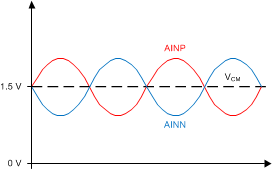
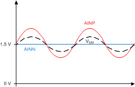
For optimum performance, drive the ADS127L01 inputs differentially, centered around a common-mode voltage of AVDD / 2. Alternatively, if the signal is of pseudo-differential nature, the negative input can be held at a constant voltage other than 0 V (typically AVDD / 2), and the voltage on the positive input can change. Figure 58 and Figure 59 show examples of both fully-differential and pseudo-differential signals, respectively.
Electrostatic discharge (ESD) diodes to AVDD and AGND protect the inputs. To prevent the ESD diodes from turning on, the absolute voltage on any input must stay within the range provided by Equation 3:
The analog input pins, AINP and AINN, at the front end of the converter are connected directly to the switched-capacitor sampling network to measure the input voltage. Figure 60 shows a conceptual diagram of the modulator circuit charging and discharging the sampling capacitor through switches, although the actual implementation is slightly different. The sampling time (tCLK / 2) is equivalent to half the master clock period, and is the inverse of the modulator sampling frequency.
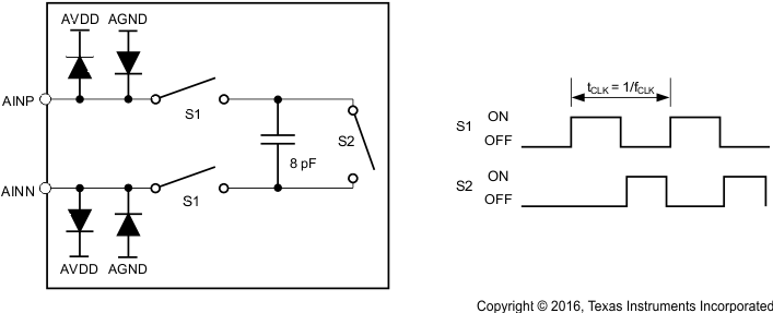 Figure 60. Equivalent Analog Input Circuitry
The average load presented by the switched-capacitor input can be modeled with an effective differential impedance, as shown in Figure 61. The effective impedance is a function of the modulator clock, and is equal to the master clock, fCLK. The ADS127L01 samples the input at very high speeds, and does not include an integrated buffer; a suitable driver must be used. See the Application and Implementation section for recommended driver circuit designs.
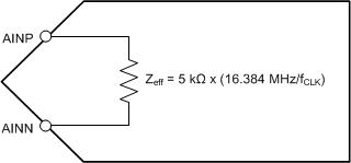 Figure 61. Effective Input Impedance
The ADC sampling network is connected to a delta-sigma modulator used to convert the analog input voltage into a data bit stream. The modulator is third-order, with a multibit quantizer that runs at the modulator clock frequency, fMOD, equal to the master clock frequency, fCLK.
8.3.2 Digital Filter
The ADS127L01 offers three selectable digital filters to perform both filtering and decimation of the digital data stream coming from the modulator. The oversampling ratio (OSR) and digital-filter selection sets the overall frequency response for the data converter. The available filter options for the ADS127L01 are:
- Low-latency sinc filter (LL)
- Wideband finite impulse response (FIR) filter with a transition band of (0.45 to 0.55) × fDATA (WB1)
- Wideband finite impulse response (FIR) filter with a transition band of (0.40 to 0.50) × fDATA (WB2)
Use the hardware FILTER[1:0] pins shown in Table 11. Each filter has four OSR options (the ratio of the modulator sampling to the output data rate, or fMOD / fDATA), shown in Table 12, that are selectable through hardware OSR[1:0] pins. The low-latency sinc filter is a cascaded sinc5 and sinc1 filter, and provides OSR options to achieve data rates ranging from 8 kSPS to 512 kSPS when operating from a 16.384-MHz master clock. The two Wideband filters use a multistage FIR topology to provide linear phase response with very low pass-band ripple and high stop-band attenuation. Wideband filters 1 and 2 provide four OSRs to achieve data rates ranging from 64 kSPS to 512 kSPS when operating from a 16.384-MHz master clock.
Select the filter and data rate when START is low, or take the START or RESET/PWDN pin low and back high after a filter-path or data-rate change. If software commands are used to control conversions, use the STOP and START commands after a change to the filter path selection or the data rate. If a conversion is in process during a filter-path or data-rate change, the output data are not valid and must be discarded.
8.3.2.1 Low-Latency Filter
The low-latency sinc filter consists of two stages: a fixed-decimation, sinc5 filter, followed by a variable-decimation, sinc1 filter. The first-stage, sinc5 digital filter decimates by a fixed value of 32. When using OSR 32, the first-stage digital filter bypasses the second filter stage, and has a sinc5 frequency response profile. The second digital-filter stage provides an additional decimation of 4, 16, or 64 to create overall decimation options of 128, 512, and 2048. Together, the two stages create four selectable, Low-latency, filter data rates when operated from a 16.384-MHz clock: 512 kSPS, 128 kSPS, 32 kSPS, and 4 kSPS.
8.3.2.1.1 Low-Latency Filter Frequency Response
The low-pass filtering effect of the sinc filter sets the overall frequency response of the ADC when in low-latency filter mode. The frequency response of OSR 32 is from only the sinc5 filter stage. The frequency response of OSR 128, 512, or 2048 is the product of the sinc5 first-stage and sinc1 second-stage frequency responses. The overall filter response is given in Equation 4:

where
- f = signal frequency
- fCLK = ADC master clock frequency = ADC modulator clock frequency
- N = Second-stage oversampling = 1 (OSR 32), 4 (OSR 128), 16 (OSR 512), or 64 (OSR 2048)
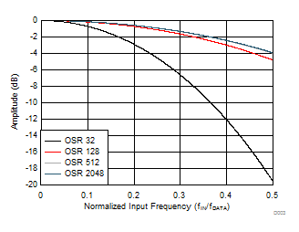
The inherent nature of the sinc filter response begins to attenuate frequencies as the signal moves away from dc. The pass band droop for inband ac signals makes the low-latency filter less ideal for ac signals.
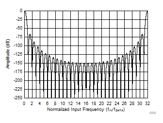
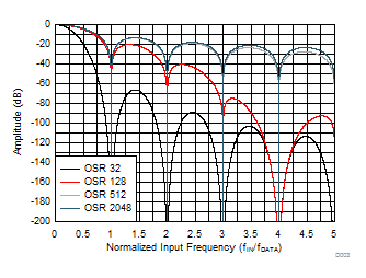
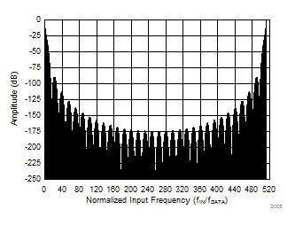
As shown in Figure 62 and Figure 63, when OSR is set to 32, the digital filter frequency response follows a sinc5 transfer function with nulls occurring at fDATA and at multiples thereof. At the null frequencies, the filter has zero gain. Convert the x-axis from the data rate, fDATA, to terms of the master clock, fCLK, by using Equation 5:
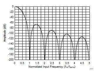
(OSR 32)
(OSR 32) to fCLK
Adjust the digital-filter response by changing the OSR or the master clock, fCLK. Noise tradeoffs are made with signal bandwidth and filter latency.
Selecting an OSR other than 32 superimposes new nulls from the second-stage sinc1 filter over the nulls produced by the sinc5 stage. The end result is a combined frequency response from a sinc5 function at OSR 32 with nulls created from the sinc1 second stage at fDATA and multiple thereof.
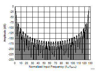
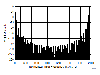
Figure 64 and Figure 65 illustrate the normalized frequency response of the Low-latency filter across all four OSR settings. OSR 32 follows a sinc5 frequency response, as highlighted in Figure 62. OSR 128, OSR 512, and OSR 2048 show a combined sinc5 and sinc1 response.
Figure 66, Figure 67, and Figure 68 illustrate the frequency response of OSR 128, OSR 512, and OSR 2048, respectively.
The Low-latency filter uses a multiple-stage, linear-phase, digital filter. Linear-phase filters exhibit constant delay time versus input frequency (also known as constant group delay). This feature of linear phase filters means that the time delay from any instant of the input signal to the corresponding same instant of the output data is constant and independent of the input-signal frequency. This behavior results in essentially zero phase error when measuring multitone signals.
(OSR 128) to fCLK
(OSR 2048) to fCLK
to 0.5 × fIN / fDATA
(OSR 512) to fCLK
8.3.2.1.2 Low-Latency Filter Settling Time
The Low-latency filter takes several conversion cycles to provide fully-settled data following a START pin low-to-high transition or a START command. The OSR setting determines the exact number of conversion cycles for first new available data, as shown in Table 3. In SPI mode, the DRDY signal remains high until settled data are available. After settled data are available, a high-to-low transition on DRDY takes place. In frame-sync mode, DOUT shifts zeroes until settled data are available. Figure 69 shows the relationship between START to the first settled available data for SPI and frame-sync interface mode. See the Start Pin (START) section for exact timing for the START pin to first available data.
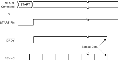 Figure 69. START to First Available Data
When applying an asynchronous step input to a converting ADS127L01, the output shift register does not gate data during digital-filter settling. The step-input-setting timing diagram shown in Figure 70 illustrates the converter step response with an asynchronous step input. The time that the analog input must be stable varies depending on the OSR. Table 3 summarizes the settling time of the Low-latency filter when a step input is applied to the input.
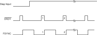 Figure 70. Asynchronous Step-Input Settling Time
Table 3. Low-Latency Filter Settling Time (Conversion Latency)
| OSR | SETTLING TIME FROM START (tCLK Periods) |
INPUT SETTLING (DRDY or FSYNC Pulses) |
|---|---|---|
| 32 | 160 | 5 |
| 128 | 288 | 3 |
| 512 | 672 | 2 |
| 2048 | 2208 | 2 |
8.3.2.2 Wideband Filter
The two Wideband filters use a multistage FIR topology to provide linear phase response with minimal pass-band ripple and high stop-band attenuation. The filters are well suited for measuring high-frequency ac signals while still maintaining excellent dc accuracy. Both Wideband filter options offer the same four OSR options; 32, 64, 128, and 256. The difference is in the transition band. When these four OSRs are paired with a 16.384-MHz clock, four selectable Wideband filter data rates are created: 512 kSPS, 256 kSPS, 128 kSPS, and 64 kSPS.
8.3.2.2.1 Wideband Filters Frequency Response
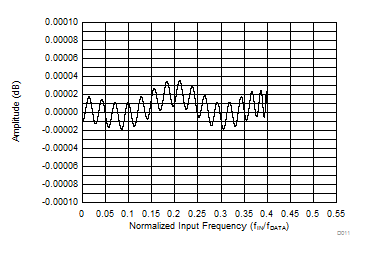
Figure 71 shows the frequency response of the Wideband 1 filter with a transition band of (0.45 to 0.55) × fDATA normalized to the output data rate, fDATA. Figure 72 shows the frequency response of the Wideband 2 filter with a transition band of (0.40 to 0.50) × fDATA normalized to the output data rate, fDATA. These plots are valid for all of the data rates available on the ADS127L01. Substitute the selected data rate, fDATA (calculated using Equation 5), to express the x-axis in absolute frequency. Figure 73 overlaps the transition band of the Wideband 1 and Wideband 2 filters, showing the difference in frequency response. The Wideband 2 filter frequency response is designed to attenuate out-of-band signals more than –116 dB by the Nyquist frequency (0.5 × fDATA) to reduce the effects of aliasing near the transition band.
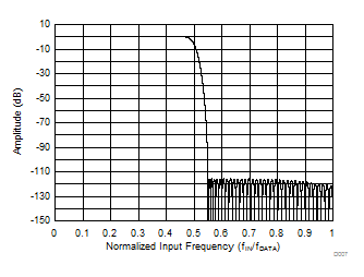
| FILTER[1:0] = 00 |
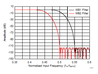
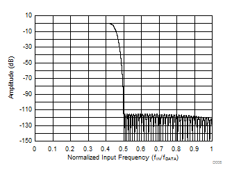
| FILTER[1:0] = 01 |
The pass-band ripple for the two digital filters are shown in Figure 74 and Figure 75.
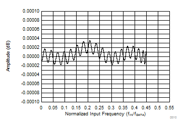
| FILTER[1:0] = 00 |
| FILTER[1:0] = 01 |
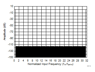
The overall frequency response repeats at the modulator sampling rate, which is the same as the input clock frequency, fCLK. Figure 76 shows the response with the fastest data rate selected (512 kSPS when fCLK = 16.384 MHz).
The Wideband filters use a multiple-stage, linear-phase, digital-filter architecture. Linear-phase filters exhibit constant delay time versus input frequency (also known as constant group delay). This feature of linear phase filters means that the time delay from any instant of the input signal to the corresponding same instant of the output data is constant and independent of the input-signal frequency. This behavior results in essentially zero phase error when measuring multitone signals.
8.3.2.2.2 Wideband Filters Settling Time
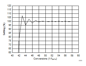
The Wideband filters fully settle before outputting data after the START pin low-to-high transition or a START command is issued. The settling time of the Wideband filters is 84 conversion cycles; the DRDY signal idles high and does not assert until new settled data are available in SPI interface mode. In frame-sync interface mode, the output shift register outputs zeroes in place of the conversion data for 84 conversion cycles until the first settled data are available. A step input on the analog input requires multiple conversions to settle if START is not pulsed, or if the START command is not issued. Figure 77 shows the settling response with the x-axis normalized to conversions or DRDY/FSYNC cycles.
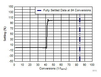
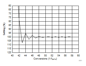
Figure 78 and Figure 79 plot the undershoot and overshoot from the Wideband digital filter during an input step function.
8.3.3 Voltage Reference Inputs (REFP, REFN)
The ADC requires the connection of an external reference voltage for operation. The voltage reference for the device is the differential voltage between REFP and REFN: VREF = (VREFP – VREFN). The reference inputs are not buffered and use a sampling structure similar to that of the analog inputs, with the equivalent circuitry on the reference inputs shown in Figure 80. The load across REFP and REFN is presented by the switched-capacitor in parallel with a 6.4-kΩ resistor, and is modeled with an effective impedance (Zeff) proportional to the master clock, fCLK, as shown in Figure 81.
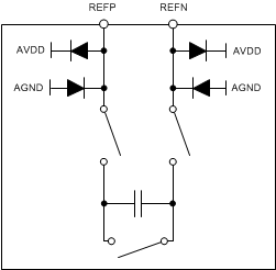 Figure 80. Equivalent Reference Input Circuitry
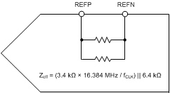 Figure 81. Effective Reference Impedance
ESD diodes protect the reference inputs. To keep these diodes from turning on, make sure the voltages on the reference pins do not go below AGND by more than 0.3 V, and do not exceed AVDD by 0.3 V. Use external Schottky clamp diodes or series resistors to limit the input current to safe values if the reference input may exceed the absolute maximum ratings (see the Absolute Maximum Ratings table).
A high-quality reference voltage with the appropriate drive strength is required for achieving the best performance from the ADS127L01. Noise and drift on the reference degrade overall system performance. Use a minimum parallel combination of 10-µF and 0.1-µF ceramic bypass capacitors directly across the reference inputs, REFP and REFN. Place these capacitors as close as possible to the device on the layout. See the Application Information section for example reference circuits.
8.3.4 Clock Input (CLK)
The ADS127L01 requires an external clock for operation. This clock signal is used for the sampling network of the modulator without any prescalers or dividers, and for the timing for the digital filter. Drive the ADC with an external clock by applying the clock input to the CLK pin. At the maximum data rate, the clock input is 16.384 MHz for HR mode, 8.192 MHz for LP mode, and 4.096 MHz for VLP mode.
A high-quality, low-jitter clock is essential for optimum performance measuring the high-frequency input signals. Any uncertainty during sampling of the input from clock jitter limits the maximum achievable SNR. For example, uses an external clock with better than 10 psrms jitter for a 200-kHz fIN. For a lower fIN, the target jitter requirement can be relaxed by –20 dB per decade. At fIN = 20 kHz, use a clock with better than 100-psrms jitter.
The selection of the external clock frequency (fCLK) does not affect the resolution of the ADS127L01. The output data rates scale with fCLK frequency down to a minimum clock frequency of fCLK = 100 kHz. Use a slower fCLK to reduce the ADC power consumption and relax the requirements of an external ADC drive circuit on the analog input and reference input.
Crystal clock oscillators are the recommended clock source. Make sure to avoid excess ringing on the clock input. A series resistor placed at the external clock buffer output often helps to reduce overshoot.
8.3.5 Out-of-Range-Detect System Monitor
An out-of-range-detect system-monitor bit (INP) is available in the status word (see the Status Word section). The out-of-range detect bit flags (INP = 1) when the input exceeds the positive or negative full-scale range, set by VREF, with each conversion result. The input is monitored using an analog comparator. The flag is issued when the full-scale range is exceeded without waiting for the conversions to propagate through the digital filter. The INP bit is used for narrow out-of-range input glitches that may or may not be removed by the ADC digital filter.
8.3.6 System Calibration
The ADC incorporates optional offset- and gain-calibration registers to system-calibrate the ADC and signal chain when in SPI interface mode. Enable the offset calibration register by setting FSC bit (bit 5 in the Configuration register) to 1, and enable the gain calibration register by setting OFC bit (bit 4 in the Configuration register) to 1. The programmable offset calibration value is 24 bits wide, and the gain calibration value is 16 bits wide. Use calibration to correct internal ADC errors or overall system errors. Calibration is only supported through direct user calibration, requiring the user to calculate and write the correction values to the calibration registers. Perform a system offset calibration before full-scale calibration. After power-up, but before calibrating, wait for the power supplies and reference voltage to fully settle.
As shown in Figure 82, the value of the offset calibration register is subtracted from the filter output, and then multiplied by the full-scale register value. The data are then clipped to a 24-bit value to provide the final output.
 Figure 82. ADC Calibration Block Diagram
Equation 6 shows the internal calibration on the data result.
The ADC offset calibration word is 24 bits, consisting of three 8-bit registers (OFC2, OFC, 1 OFC0), as shown in Table 4. The offset value is twos complement format with a maximum positive value equal to 7FFFFFh (for negative offset), and a maximum negative value equal to 800000h (for positive offset). A register value equal to 000000h has no offset correction. For offset calibration, short the ADC inputs or system inputs, and average the conversions; averaging reduces noise for a more accurate calibration. Write the average value to the offset calibration registers. The ADC subtracts the value from the conversion result.
Table 4. Offset Calibration Registers
| REGISTER | BYTE ORDER | ADDRESS | BIT ORDER | |||||||
|---|---|---|---|---|---|---|---|---|---|---|
| OFC0 | LSB | 02h | OFC_B7 | OFC_B6 | OFC_B5 | OFC_B4 | OFC_B3 | OFC_B2 | OFC_B1 | OFC_B0 (LSB) |
| OFC1 | MID | 03h | OFC_B15 | OFC_B14 | OFC_B13 | OFC_B12 | OFC_B11 | OFC_B10 | OFC_B9 | OFC_B8 |
| OFC2 | MSB | 04h | OFC_B23 (MSB) | OFC_B22 | OFC_B21 | OFC_B20 | OFC_B19 | OFC_B18 | OFC_B17 | OFC_B16 |
The ADC gain calibration word is 16 bits consisting of two 8-bit registers (FSC1, FSC0), as shown in Table 5. The full-scale calibration value is twos compliment, with a unity-gain correction factor at a register value equal to 8000h. Table 6 shows register values for selected gain factors.
Table 5. Gain Calibration Registers
| REGISTER | BYTE ORDER | ADDRESS | BIT ORDER | |||||||
|---|---|---|---|---|---|---|---|---|---|---|
| FSC0 | LSB | 05h | FSC_B7 | FSC_B6 | FSC_B5 | FSC_B4 | FSC_B3 | FSC_B2 | FSC_B1 | FSC_B0 (LSB) |
| FSC1 | MSB | 06h | FSC_B15 (MSB) | FSC_B14 | FSC_B13 | FSC_B12 | FSC_B11 | FSC_B10 | FSC_B9 | FSC_B8 |
Table 6. Gain Calibration Register Values
| FSCAL[2:0] REGISTER VALUE | GAIN FACTOR |
|---|---|
| 7FFFh | 2.00 |
| 8000h | 1.00 |
| 0000h | 0.00 |
For gain calibration, apply a dc calibration voltage that is less than positive full-scale voltage in order to avoid clipped codes (VIN < +FSR), and average the conversions to reduce noise for a more accurate calibration. Gain calibration is computed as shown in Equation 7, after offset error is removed.
If the actual code is higher than the expected value, then the calculated calibration value is less than 8000h, and the ADC gain is subsequently reduced. Write the calibration value to the gain calibration registers.
8.4 Device Functional Modes
8.4.1 Operating Modes (HR, LP, VLP)
The ADS127L01 offers three operational modes: high-resolution (HR), low-power (LP), and very-low-power (VLP). These modes optimize power consumption by restricting the maximum master-clock frequency (fCLK) controlling the data rate. The status of the HR pin determines if the device is in HR mode or LP mode. Enter VLP mode by setting the ADS127L01 in LP mode, and increasing the value of the external REXT power scaling resistor from 60.4 kΩ to 120 kΩ. The tolerance on the REXT power-scaling resistor must be 1% or better. The analog current consumed by AVDD and LVDD decreases when in LP mode, and decreases further in VLP mode, with a tighter restriction on maximum master-clock frequency. Table 7 details the HR pin and REXT settings for each operating mode in the ADS127L01.
Table 7. Operating Mode Selection
| OPERATING MODE | OPERATING MODE SELECTION PIN (HR) | REXT VALUE | MAXIMUM fCLK |
|---|---|---|---|
| High-Resolution (HR) | 1 | 60.4 kΩ | 17.6 MHz |
| Low-Power (LP) | 0 | 60.4 kΩ | 8.8 MHz |
| Very-Low-Power (VLP) | 0 | 120 kΩ | 4.4 MHz |
8.4.2 Hardware Mode Pins
The ADS127L01 uses two-state hardware mode pins for ADC configuration. The operating mode, interface selection, digital filter selection, and oversampling ratio (OSR) are all controlled through hardware pins. These pins are constantly monitored, and set by either pulling them high to DVDD, or low to DGND. Use pull-up or pull-down 100-kΩ resistors, or directly tie the pins to microcontroller or DSP I/O lines to set the state of the pins. When a change is sensed on the hardware mode pins after power-up, the ADC automatically issues a reset. To ensure synchronization, issue a software reset command, or pulse the RESET/PWDN pin following the mode change delay, td(MD).
When using the SPI interface mode, DRDY is held high after a mode change occurs until settled data are ready; see Figure 83 and Table 8.
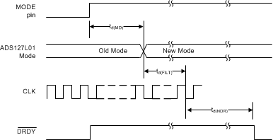 Figure 83. Mode Change Timing (SPI Interface)
Table 8. SPI Interface New Data After Mode Change
| SYMBOL | DESCRIPTION | MIN | TYP | MAX | UNIT | |
|---|---|---|---|---|---|---|
| td(MD) | Delay time, MODE pin rising edge to mode change | 3 | tCLK | |||
| td(FILT) | Delay time, mode change to first modulator sample | 3.5 | 4.5 | tCLK | ||
| td(NDR) | Delay time for new data to be ready | Wideband filters | 84 | tDATA | ||
| Low-latency filter | See Table 3 | tDATA | ||||
In Frame-sync intreface mode, the DOUT pins are held low after a mode change occurs until settled data are ready; see Figure 84 and Table 9. Data can be read from the device to detect when DOUT changes, indicating that data are valid.
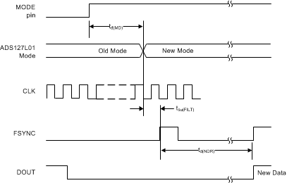 Figure 84. Mode Change Timing (Frame-Sync Interface)
Table 9. Frame-Sync Interface New Data After Mode Change
| SYMBOL | DESCRIPTION | MIN | TYP | MAX | UNIT | |
|---|---|---|---|---|---|---|
| td(MD) | Delay time, MODE pin rising edge to mode change | 3 | tCLK | |||
| tsu(FILT) | Setup time, mode change to FSYNC rising edge | Frame-sync slave | 5 | tCLK | ||
| Frame-sync master | 1 | tCLK | ||||
| td(NDR) | Delay time for new data to be ready | Wideband filters | 84 | tDATA | ||
| Low-latency filter | See Table 3 | tDATA | ||||
8.4.2.1 Interface Selection Pins (FORMAT, FSMODE)
Data are read from the ADS127L01 using one of two selectable interface modes, SPI or frame-sync. Use the FORMAT input pin to select among the two interface options.
If the frame-sync interface is selected, the ADS127L01 offers either a master or slave option, selectable using the FSMODE pin. Table 10 lists the available options.
Table 10. Interface Mode Options
| FORMAT | FSMODE | INTERFACE MODE |
|---|---|---|
| 0 | 0 | SPI |
| 0 | 1 | SPI |
| 1 | 0 | Frame-sync slave mode |
| 1 | 1 | Frame-sync master mode |
8.4.2.2 Digital-Filter Path Selection Pins (FILTER[1:0])
Three digital filter options are available in the ADS127L01: two Wideband filter options, and a Low-latency filter. See the Digital Filter section for detailed information on the digital filters and the frequency responses. The FILTER[1:0] hardware mode pins set the filter path selection for the modulator data, as shown in Table 11. Select the filter when START is low, or take the START or RESET/PWDN pin low and back high after a filter path change. If software commands are used to control conversions, use the STOP and START commands after a change to the filter path selection. If a conversion is in process during a filter path change, the output data are not valid and must be discarded.
Table 11. Digital-Filter Path Selection
| FILTER1 | FILTER0 | SELECTED FILTER PATH | FILTER TRANSITION BAND |
|---|---|---|---|
| 0 | 0 | Wideband 1 filter | 0.45 × fDATA to 0.55 × fDATA |
| 0 | 1 | Wideband 2 filter | 0.40 × fDATA to 0.50 × fDATA |
| 1 | 0 | Low-latency filter | SINC5 / SINC |
| 1 | 1 | Reserved: do not use | |
8.4.2.3 Oversampling Ratio Selection Pins (OSR[1:0])
The ADS127L01 has two hardware oversampling ratio (OSR) pins used to configure the converter data rate. The rate at which the modulator bit stream data is decimated differs depending on whether the Wideband or the Low-latency digital filter is used (set using the Digital-Filter Path Selection Pins (FILTER[1:0])). The OSR options and corresponding maximum data rate at fCLK = 16.384 MHz are shown in Table 12 for both the Wideband and the Low-latency filters. Change the OSR when START is low, or take the START or RESET/PWDN pin low and back high after changing the OSR. If software commands are used to control conversions, use the STOP and START commands after changing the OSR.
Table 12. OSR Selection
| FILTER | OSR1 | OSR0 | OSR | DATA RATE (kSPS) AT fCLK = 16.384 MHz |
|---|---|---|---|---|
| Wideband filters | 0 | 0 | 32 | 512 |
| 0 | 1 | 64 | 256 | |
| 1 | 0 | 128 | 128 | |
| 1 | 1 | 256 | 64 | |
| Low-latency filter | 0 | 0 | 32 | 512 |
| 0 | 1 | 128 | 128 | |
| 1 | 0 | 512 | 32 | |
| 1 | 1 | 2048 | 8 |
8.4.3 Start Pin (START)
The START pin controls the start and stop of ADC conversions used for converter synchronization. Take the START pin low to stop conversions and reset the digital filter. Pull START high to start or restart the conversions.
Synchronization allows the conversion to be aligned with an external event, such as the changing of an external multiplexer on the analog inputs. The START pin is also used to synchronize multiple devices to within the same CLK cycle.
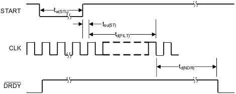
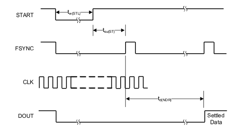
Figure 85 and Figure 86 illustrate the timing requirement for the START pin with respect to CLK in SPI and frame-sync interface modes. After synchronization, indication of valid data depends on whether SPI or frame-sync interface mode is used.
In the SPI interface mode, DRDY goes high as soon as START is taken low, as shown in Figure 85. After START is returned high, DRDY stays high while the digital filter completes reset and settles. After valid data are ready for retrieval, DRDY goes low.
Table 13. SPI Interface Start
| SYMBOL | DESCRIPTION | MIN | TYP | MAX | UNIT | |
|---|---|---|---|---|---|---|
| tw(STL) | Pulse duration, START low | 4 | tCLK | |||
| tsu(ST) | Setup time, START rising edge to CLK rising edge | 10 | ns | |||
| td(FILT) | Delay time, START rising edge to first modulator sample | 4 | 5 | tCLK | ||
| td(NDR) | Delay time for new data to be ready | Wideband filters | 84 | tDATA | ||
| Low-latency filter | See Table 3 | tDATA | ||||
In frame-sync interface, DOUT goes low as soon as START is taken low, as shown in Figure 86. After START is returned high, the following FSYNC rising edge releases the digital filter from reset to begin conversions. DOUT stays low while the digital filter is settling. Data are ready for retrieval on DOUT after the digital filter settles. For proper synchronization, FSYNC, SCLK, and CLK must be established before taking START high, and must then remain running. If either CLK, FSYNC or SCLK are interrupted or reset, reassert the START pin.
Table 14. Frame-Sync Interface Start
| SYMBOL | DESCRIPTION | MIN | TYP | MAX | UNIT | |
|---|---|---|---|---|---|---|
| tw(STL) | Pulse duration, START low | 4 | tCLK | |||
| tsu(ST) | Setup time, START rising edge to FSYNC rising edge | Frame-sync slave | 6 | tCLK | ||
| Frame-sync master | 5 | tCLK | ||||
| td(NDR) | Delay time for new data to be ready | Wideband filters | 84 | tDATA | ||
| Low-latency filter | See Table 3 | tDATA | ||||
In addition to the START pin, START and STOP commands are also available to control the start and stop of conversions, but only when using the SPI interface. Using the commands requires that the hardware START pin is tied low the entire time. The START command is also used to synchronize multiple ADS127L01s sharing the same SPI interface. See the SPI Commands section for information on using the START and STOP commands to control ADC conversions.
8.4.4 Reset and Power-Down Pin (RESET/PWDN)
The RESET/PWDN pin has two functions, depending on the amount of time the pin is held in a low state. If RESET/PWDN is low for < 215 – 1 CLK periods, the ADS127L01 resets both the digital filter and register contents to default settings. The low-to-high transition of the RESET/PWDN pin brings the ADS127L01 out of reset by completing the digital filter reset, as shown in Figure 87 and Figure 88.
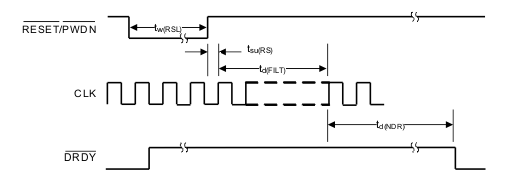 Figure 87. Reset Timing (SPI Interface)
Table 15. SPI Interface Reset Timing
| SYMBOL | DESCRIPTION | MIN | TYP | MAX | UNIT | |
|---|---|---|---|---|---|---|
| tw(RSL) | Pulse duration RESET/PWDN low | 4 | 215 – 1 | tCLK | ||
| tsu(RS) | Setup time, RESET/PWDN rising edge to CLK rising edge | 10 | ns | |||
| td(FILT) | Delay time, RESET/PWDN rising edge to first modulator sample | 37 | tCLK | |||
| td(NDR) | Delay time for new data to be ready | Wideband filters | 84 | tDATA | ||
| Low-latency filter | See Table 3 | tDATA | ||||
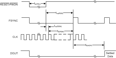 Figure 88. Reset Timing (Frame-Sync Interface)
Table 16. Frame-Sync Interface Reset Timing
| SYMBOL | DESCRIPTION | MIN | TYP | MAX | UNIT | |
|---|---|---|---|---|---|---|
| tw(RSL) | Pulse duration RESET/PWDN low | 4 | 215 – 1 | tCLK | ||
| tsu(RSS) | Frame-Sync Slave Mode: Setup time, RESET/PWDN rising edge to first FSYNC | 7 | tCLK | |||
| tsu(RSM) | Frame-Sync Master Mode: Setup time, RESET/PWDN rising edge to CLK rising edge | 10 | ns | |||
| td(RSM) | Frame-Sync Master Mode: Delay time, CLK rising edge to FSYNC rising edge | 4 | tCLK | |||
| td(NDR) | Delay time for new data to be ready | Wideband filters | 84 | tDATA | ||
| Low-latency filter | See Table 3 | tDATA | ||||
If RESET/PWDN is low for > 215 – 1 CLK periods, the ADS127L01 enters power-down mode where both the analog and digital circuitry is completely deactivated. The digital inputs are internally disabled so there is no concern in driving the pins.
Use individual 1-MΩ pull-down resistors placed on CAP3 to DGND, SCLK to DGND, and DRDY/FSYNC to DGND if power-down mode is planned to be used. These resistors help discharge voltage when the device is placed in power-down mode. Shut down the CLK and SCLK in power-down mode to avoid additional power consumption.
Return the RESET/PWDN pin high to exit power-down mode. As shown in Figure 89 and Figure 90, a minimum of 215 + 37 master clock periods must elapse before the device exits power-down mode and begins sampling when using SPI interface mode. DRDY stays high after exiting power-down mode while the digital filter settles.
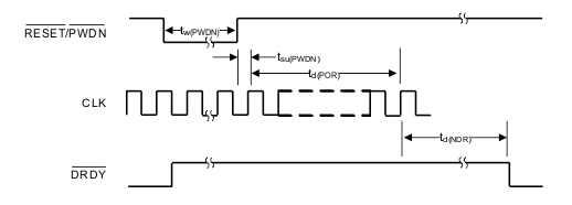 Figure 89. Power-Down Timing (SPI Interface)
Table 17. SPI Interface Power-Down Timing
| SYMBOL | DESCRIPTION | MIN | TYP | MAX | UNIT | |
|---|---|---|---|---|---|---|
| tw(PWDN) | Pulse duartionRESET/PWDN low | 215 | tCLK | |||
| tsu(PWDN) | Setup time, RESET/PWDN rising edge to CLK rising edge | 10 | ns | |||
| td(POR) | Delay time, power-on-reset complete following RESET/PWDN rising edge | 215 + 37 | tCLK | |||
| td(NDR) | Delay time for new data to be ready | Wideband filters | 84 | tDATA | ||
| Low-latency filter | See Table 3 | tDATA | ||||
A minimum of 215 + 7 master clock periods must elapse before the device exits power-down mode to begin sampling, when in Frame-Sync interface mode, as shown in Figure 90 and Table 18. When using Frame-Sync interface mode, DOUT will read back low while the digital filter settles.
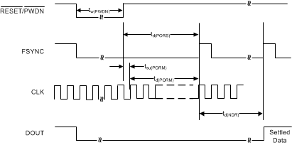 Figure 90. Power-Down Timing (Frame-Sync Interface)
Table 18. Frame-Sync Interface Power-Down Timing
| SYMBOL | DESCRIPTION | MIN | TYP | MAX | UNIT | |
|---|---|---|---|---|---|---|
| tw(PWDN) | Pulse duration RESET/PWDN low | 215 | tCLK | |||
| td(PORS) | Frame-Sync Slave Mode, Delay time, RESET/PWDN rising edge to FSYNC rising edge | 215 + 7 | tCLK | |||
| tsu(PORM) | Frame-Sync Slave Mode, Setup time, RESET/PWDN rising edge to CLK rising edge | 10 | ns | |||
| td(PORM) | Frame-Sync Slave Mode, Delay time, CLK rising edge to FSYNC rising edge | 215 + 7 | tCLK | |||
| td(NDR) | Delay time for new data to be ready | Wideband filters | 84 | tDATA | ||
| Low-latency filter | See Table 3 | tDATA | ||||
8.5 Programming
Data are retrieved from the ADS127L01 using a serial interface. To provide easy connection to either microcontrollers or DSPs, three communication modes are available: SPI, frame-sync master, and frame-sync slave. The FORMAT and FSMODE hardware mode pins select the interface. The same communication pins are used for all three interfaces: SCLK, DRDY/FSYNC, DIN, DAISYIN, and DOUT; however, functionality depends on the interface selected.
When FORMAT = 0, SPI interface is selected, and the DRDY/FSYNC pin becomes a data ready (DRDY) output. In SPI interface mode, commands and internal registers are available for further device configuration. Tie the FSMODE pin to DGND when using SPI communication mode.
When FORMAT = 1, frame-sync interface mode is selected, and the DRDY/FSYNC pin becomes an FSYNC input or output. Frame-sync offers two different modes controlled by the FSMODE pin.
When FSMODE = 0, the interface uses frame-sync slave mode, requiring that the SCLK and FSYNC signals are driven by the processor to the ADS127L01.
When FSMODE = 1, the interface is set to frame-sync master mode, and the SCLK and FSYNC signals are generated from the ADC derived from the master clock.
8.5.1 Serial Peripheral Interface (SPI) Programming
The SPI-compatible serial interface of the device is used to read conversion data, read and write the device configuration registers, and control device operation. Only SPI mode 1 (CPOL = 0, CPHA = 1) is supported. The interface consists of five control lines (CS, SCLK, DIN, DOUT, and DRDY/FSYNC), but the interface is operational with only four control lines. If the serial bus is not shared with any other device, CS can be tied low permanently so that only signals SCLK, DIN, DOUT and DRDY/FSYNC are required to communicate with the device.
8.5.1.1 Chip Select (CS)
Chip select (CS) is an active-low input that selects the device for SPI communication. CS must remain low for the entire duration of the serial communication to complete a command or data readback. When CS is taken high, the serial interface is reset, SCLK is ignored, and DOUT enters a high-impedance state. If the serial bus is not shared with another peripheral, CS can be tied low.
8.5.1.2 Serial Clock (SCLK)
The serial clock (SCLK) features a Schmitt-triggered input, and is used to clock data into and out of the device on DIN and DOUT, respectively. SCLKs can be sent to the ADC continuously or in byte increments. Even though the input has hysteresis, keep the SCLK signal as clean as possible to prevent glitches from accidentally shifting data. When the serial interface is idle, hold SCLK low.
8.5.1.3 Data Ready (DRDY/FSYNC)
In SPI interface mode, DRDY/FSYNC is an active-low, new-data-ready indicator for when a new conversion result is ready for retrieval. When DRDY/FSYNC transitions low, new conversion data are ready. The DRDY/FSYNC signal transitions from low to high with the first SCLK falling edge, as shown in Figure 91. When no data are read during continuous conversion mode, DRDY/FSYNC remains low but pulses high for a duration of 2 · tCLK before the next DRDY/FSYNC falling edge. The DRDY/FSYNC pin is always actively driven, even when CS is high.
A new conversion result is loaded into the output shift register before DRDY transitions from high to low. The LSB of the previous data word must be read at least 4 · tCLK before the next DRDY falling edge. This delay is known as keep-out time (tKO). Keep SCLK low during tKO until the next conversion result is ready for retrieval, as shown in Figure 91.
8.5.1.4 Data Input (DIN)
The data input pin (DIN) is used with SCLK to send data (commands and register data) to the device. The device latches data on DIN on the SCLK falling edge. The device never drives the DIN pin.
8.5.1.5 Data Output (DOUT)
DOUT is used with SCLK to read conversion and register data from the device. Data on DOUT are shifted out on the SCLK rising edge, to be read from the host on the SCLK falling edge. DOUT goes to a high-impedance state when CS is high.
8.5.1.6 Daisy-Chain Input (DAISYIN)
DAISYIN is an optional pin used with SCLK to shift data in from a secondary ADS127L01 device when in a daisy-chain configuration. Data are shifted out from DOUT of a secondary device into the DAISYIN pin of the first device. The individual data bits are latched into DAISYIN on the SCLK falling edge. See the Multiple Device Configuration section for more information on using daisy-chain mode. If not used, tie the DAISYIN pin to DGND.
8.5.1.7 SPI Timeout
The ADS127L01 offers an SPI timeout feature that is used to recover communication when a serial interface transmission is interrupted. This feature is especially useful in applications where CS is permanently tied low and is not used to frame a communication sequence.
The timeout feature is disabled by default, but can be enabled in the CONFIG register. The time for the timeout to issue is also configurable using the CONFIG register. When enabled, and whenever a complete command is not sent within 214 · tCLK or 216 · tCLK (configurable by the TOUT_DEL bit in the CONFIG register), the serial interface resets and the next SCLK pulse starts a new communication cycle. For the RREG and WREG commands, a complete command includes the command byte plus the register bytes that are read or written.
8.5.1.8 SPI Commands
The ADS127L01 provides flexible configuration, including commands and configurable registers, only when using the SPI interface. The commands, summarized in Table 19, are stand-alone and configure the operation of the ADS127L01. Each command is a single byte, except for the register read and write operations that require two or more bytes. CS must remain low for the entire command operation (especially for multibyte commands). Take CS high during a opcode command to abort the command.
Table 19. Command Definitions
| COMMAND | DESCRIPTION | FIRST BYTE | SECOND BYTE |
|---|---|---|---|
| System Commands | |||
| RESET | Reset the device | 0000 011x | |
| START | Start or restart (synchronize) conversions | 0000 100x | |
| STOP | Stop conversion | 0000 101x | |
| Data Read Commands | |||
| RDATA | Read data by command | 0001 0010 | |
| Register Commands | |||
| RREG | Read (nnnn + 1) registers starting at address rrrr | 0010 rrrr | 0000 nnnn |
| WREG | Write (nnnn + 1) registers starting at address rrrr | 0100 rrrr | 0000 nnnn |
8.5.1.8.1 RESET (0000 011x)
The RESET command halts conversions and resets the ADC to power-on-reset values. During this time, the digital filter resets, requiring an additional power-up time for conversions to begin. The RESET command is decoded by the ADS127L01 on the seventh falling edge of SCLK. For more information, refer to the Reset and Power-Down Pin (RESET/PWDN) section.
8.5.1.8.2 START (0000 100x)
The START command starts conversions and resynchronize the device. When conversions are stopped, either at power-up or following a STOP command, issue a START command to begin ADC conversions. Issuing a START command restarts the conversions by resetting the digital filters. During the reset period, DRDY/FSYNC does not toggle. The START command is decoded by the ADS127L01 on the seventh falling edge of SCLK. The START pin must be held low if the START and STOP commands are used. For more information, refer to the Start Pin (START) section.
8.5.1.8.3 STOP (0000 101x)
The STOP command places the ADC in an idle state where the modulator stops converting. The STOP command is decoded by the ADS127L01 on the seventh falling edge of SCLK. The START pin must be held low if the START and STOP commands are used.
8.5.1.8.4 RDATA (0001 0010)
The RDATA command reloads the output shift register to the MSB of the most recent data. The RDATA command is decoded on the eighth SCLK falling edge, and begins shifting out the MSB of the data word on DOUT on the ninth SCLK.
8.5.1.8.5 RREG (0010 rrrr 0000 nnnn)
The RREG command reads the number of bytes specified by nnnn (number of registers to be read – 1) from the device configuration register, starting at register address rrrr. The command is completed after nnnn + 1 bytes are clocked out after the RREG command byte. For example, the command to read three registers (nnnn = 0010) starting at register address 00h (rrrr = 0000) is 0010 0000 0000 0010 as shown in Figure 92. The communication length must be extended by the proper number of SCLKs to shift register contents out.
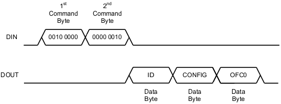 Figure 92. Read from Register
8.5.1.8.6 WREG (0100 rrrr 0000 nnnn)
The wREG command writes the number of bytes specified by nnnn (number of registers to be written – 1) to the device configuration register, starting at register address rrrr. The command is completed after nnnn + 1 bytes are clocked in after the WREG command byte. For example, the command to write two registers (nnnn = 0001) starting at register address 01h (rrrr = 0001) is 0100 0001 0000 0001 as shown in Figure 93. Two bytes follow the command to write the contents to the registers. The frame must extend by the proper number of SCLKs to write data to the registers.
 Figure 93. Write to Register
8.5.2 Frame-Sync Programming
Frame-sync interface is similar to the interface often used on audio ADCs. The ADS127L01 offers both frame-sync master and frame-sync slave modes that are selectable using the FSMODE pin. In frame-sync format, commands and register assignments are not available. Tie DIN low to DGND.
8.5.2.1 Frame-Sync Master Mode
When operating in frame-sync master mode, the ADC acts as the system master, and provides the FSYNC, SCLK, and DOUT signals. The FSYNC and SCLK signals are derived as a function of the master clock input, fCLK. The data are output MSB first on the rising edge of FSYNC.
8.5.2.1.1 Chip Select (CS) in Frame-Sync Master Mode
CS is not used in frame-sync interface mode.. Tie the CS pin to DGND.
8.5.2.1.2 Serial Clock (SCLK) in Frame-Sync Master Mode
When operating in frame-sync master mode, the serial clock (SCLK) is derived from the master clock and provided from the ADC to the microprocessor. Every frame period, tc(FRAME), includes 32 SCLKs to shift all data out before new data are ready. This SCLK speed is proportional to the frame size, tc(FRAME) / 32 in frame-sync master mode. The frame size is determined by the data rate setting using the hardware FILTER pin settings, OSR pin settings, and speed of the master clock, fCLK. The data on DOUT are clocked out on the falling edge of SCLK to be latched by the host processor on the rising edge of SCLK.
8.5.2.1.3 Frame-Sync (DRDY/FSYNC) in Frame-Sync Master Mode
In frame-sync master mode, the FSYNC pin is an output whose period is proportional to the ADC programmed data rate. Within each FSYNC period are 32 SCLKs to shift out the data on DOUT. The FSYNC duty cycle is designed to be 50-50, where an FSYNC low-to-high transition takes place before the MSB of new data, and high-to-low transition takes place before bit 15 on the falling edge of SCLK. For more information on FSYNC master-mode timing, see the Frame-Sync Master Mode Timing Requirements.
8.5.2.1.4 Data Input (DIN) in Frame-Sync Master Mode
DIN is not available in frame-sync master mode. Tie DIN to DGND.
8.5.2.1.5 Data Output (DOUT) in Frame-Sync Master Mode
The conversion data are clocked out on the falling edge of SCLK to be latched by the host processor on the rising edge of SCLK. The MSB data become valid on DOUT after FSYNC goes high. The subsequent bits are shifted out with each falling edge of SCLK.
8.5.2.1.6 Daisy-Chain Input (DAISYIN) in Frame-Sync Master Mode
DAISYIN and daisy-chain operation are not supported in frame-sync master mode. Tie DAISYIN to DGND.
8.5.2.2 Frame-Sync Slave Mode
When operating in frame-sync slave mode, the user must supply the framing signal FSYNC (similar to the left/right clock on stereo audio ADCs) and the serial clock SCLK (similar to the bit clock on audio ADCs). The data are output MSB first or left-justified on the rising edge of FSYNC. The FSYNC and SCLK inputs must be continuously running with the relationships shown in the Frame-Sync Timing Requirements.
8.5.2.2.1 Chip Select (CS) in Frame-Sync Slave Mode
CS is not used in frame-sync programming. Tie CS to DGND.
8.5.2.2.2 Serial Clock (SCLK) in Frame-Sync Slave Mode
In frame-sync slave mode, use SCLK to clock data out on DOUT. SCLK must run continuously; if SCLK is shut down, the data read back is corrupted. The number of SCLKs within a frame period (tc(FRAME)) can be any power-of-two ratio of CLK cycles (1, 1/2, 1/4, and so on), as long as the number of cycles is sufficient to shift the data output within one frame.
Use SCLK to also shift data into DAISYIN when multiple devices are configured for daisy-chain operation. Even though SCLK has hysteresis, keep SCLK as clean as possible to prevent glitches from accidentally shifting the data.
8.5.2.2.3 Frame-Sync (DRDY/FSYNC) in Frame-Sync Slave Mode
In frame-sync slave mode, the FSYNC pin is an input that transitions low to high at the data-rate frequency. The required number of fCLK cycles to each FSYNC period depends on the configuration of the FILTER[1:0] and OSR[1:0] pins. If the FSYNC period is not the proper value, data read back is corrupted. For more information on frame-sync slave-mode timing, see the Frame-Sync Slave Mode Timing Requirements.
8.5.2.2.4 Data Input (DIN) in Frame-Sync Slave Mode
DIN is not used in frame-sync slave mode. Tie the DIN pin to DGND.
8.5.2.2.5 Data Output (DOUT) in Frame-Sync Slave Mode
The conversion data are clocked out on the falling edge of SCLK to be latched by the host processor on the rising edge of SCLK. The MSB data become valid on DOUT after FSYNC goes high. The subsequent bits are shifted out with each falling edge of SCLK.
8.5.2.2.6 Daisy-Chain Input (DAISYIN) in Frame-Sync Slave Mode
DAISYIN is an optional pin used along with SCLK to shift data from a secondary ADS127L01 device. Data are shifted out from DOUT of a secondary device into the DAISYIN pin of the first device. The data on DOUT is latched into DAISYIN on the SCLK falling edge. See the Multiple Device Configuration section for more information on using daisy-chain mode. Tie the DAISYIN pin to DGND if not used.
8.5.3 Data Format
The ADS127L01 provides either a 24-bit or 32-bit output word, 24 bits of which are data in binary twos complement format with an optional eight LSBs containing status word information. The size of one code (LSB) is calculated using Equation 8:
A positive full-scale input [VIN ≥ (+FS – 1 LSB) = (VREF – 1 LSB)] produces an output code of 7FFFFFh, and a negative full-scale input (VIN ≤ –FS = –VREF ) produces an output code of 800000h. The output clips at these codes for signals that exceed full-scale.
Table 20 summarizes the ideal output codes for different input signals.
Table 20. Ideal Output Code Versus Input Signal
| INPUT SIGNAL, VIN
(VAINP – VAINN) |
IDEAL OUTPUT CODE(1) |
|---|---|
| ≥ +FS (223 – 1) / 223 | 7FFFFFh |
| +FS / 223 | 000001h |
| 0 | 0 |
| –FS / 223 | FFFFFFh |
| ≤ –FS | 800000h |
8.5.4 Status Word
Trailing the 24 bits of data is an optional 8-bit status word. The status word provides a real-time update of internal system monitors and data integrity. By default, the contents are a mixture of 4-bit CRC data integrity and system monitors. Alternatively, the status word can be set to output an 8-bit CRC without the system monitors. The CRCB bit in the CONFIG regsiter controls the status word contents. Set the CRCB bit to 0 for the status word to contain 4-bit CRC [bits 7:4], one bit [bit 3] to monitor out of range input (INP), and three bits [bits 2:0] to read back as 0. Set the CRCB bit to 1 for all eight bits [bits 7:0] of the status word to contain 8-bit CRC. See Figure 94 for a visual representation of the two modes.
By default, the optional 8-bit status word is enabled, but can be disabled when operating in SPI interface mode and setting the CS_ENB bit to 1 in the CONFIG register.
 Figure 94. Status Word
8.5.5 Cyclic Redundancy Check (CRC)
The ADS127L01 implements two standard CRC algorithms: CRC-4-ITU to provide a 4-bit CRC, and CRC-8-CCITT for an 8-bit CRC. By default, the CRC-4-ITU option is enabled. Set the CRCB bit to 1 in the CONFIG register to change the format to CRC-8-CCITT and remove the system monitor bits from the status word.
The CRC is placed after the ADC data. The CRC is calculated using only the ADC output. When the 4-bit CRC is enabled, the ADS127L01 outputs a 4-bit status block after the CRC that is not used as part of the CRC check.
8.5.5.1 Computing the CRC
To calculate the CRC, divide the data bytes by the CRC polynomial using an XOR operation.
In 4-bit CRC mode, the CRC value is the 4-bit remainder of the division of the data bytes by a CRC polynomial of P(x) = x4 + x + 1.
In 8-bit CRC mode, the CRC value is the 8-bit remainder of the division of the ADC data bytes by a CRC polynomial of P(x) = x8 + x2 + x + 1.
Then compare the calculated CRC values to the provided CRC value in the ADC output.
If the values do not match, a data-transmission error has occurred. In the event of a data-transmission error, read the data again. The CRC provides a higher level of detection of multiple-bit errors.
The following list shows a general procedure to compute the CRC value. Assume the shift register is n bits wide, where n is the number of CRC bits:
- Set the polynomial value to 0x3 for an 4-bit CRC, or 0x07 for an 8-bit CRC .
- Set the shift register to all zeros.
- Begin with the MSB in the data stream. For every n bits:
- Align the MSB of the data stream with the MSB of the shift register. XOR the data with the shift register, and place the result in the shift register.
- Test the MSB of the shift register n times, and do one of the following each time:
- If the most significant bit of the shift register is set, shift the register left by one bit, XOR the result with the polynomial, and place the result into the shift register.
- If the most significant bit of the shift register is not set, shift the register left by one bit.
- The result in the shift register is the CRC check value.
NOTE
The CRC algorithm used here employs an assumed set high bit. This bit is divided out by left-shifting the bit out of the register prior to XORing with the polynomial shift register. This process allows for calculation of the CRC with 8-bit hardware.
8.6 Register Maps
Table 21 describes the various ADS127L01 registers. Access to the registers is available in SPI interface mode. Register access is not available in frame-sync master or slave interface modes.
Table 21. ADS127L01 Register Assignments
| ADDRESS | REGISTER | RESET VALUE (Hex) | BIT 7 | BIT 6 | BIT 5 | BIT 4 | BIT 3 | BIT 2 | BIT 1 | BIT 0 |
|---|---|---|---|---|---|---|---|---|---|---|
| Device ID (Read-Only Registers) | ||||||||||
| 00h | ID | x3h(1) | REV_ID[4:0] | DEV_ID[2:0] | ||||||
| Configuration Settings | ||||||||||
| 01h | CONFIG | 00h | 0 | 0 | FSC | OFC | TOUT_DEL | SPI_TOUT | CS_ENB | CRCB |
| 02h | OFC0 | 00h | OFC_B[7:0] | |||||||
| 03h | OFC1 | 00h | OFC_B[15:8] | |||||||
| 04h | OFC2 | 00h | OFC_B[23:16] | |||||||
| 05h | FSC0 | 00h | FSC_B[7:0] | |||||||
| 06h | FSC1 | 80h | FSC_B[15:8] | |||||||
| Device Settings (Read-Only Registers) | ||||||||||
| 07h | MODE | xx(1) | 0 | HR | OSR[1:0] | OSR[1:0] | FILTER[1:0] | FILTER[1:0] | FORMAT | FSMODE |
8.6.1 ID: ID Control Register (address = 00h) [reset = x3h]
This register is programmed during device manufacture to indicate device characteristics.
| 7 | 6 | 5 | 4 | 3 | 2 | 1 | 0 |
| REV_ID[4:0] | DEV_ID[2:0] | ||||||
| R-Undefined(1) | R-3h | ||||||
| LEGEND: R/W = Read/Write; R = Read only; -n = value after reset |
Table 22. ID Register Field Descriptions
| Bit | Field | Type | Reset | Description |
|---|---|---|---|---|
| 7:3 | REV_ID[4:0] | R | xh(1) | Revision ID. These bits indicate the revision of the device and are subject to change without notice. |
| 2:0 | DEV_ID[2:0] | R | 3h | Device Family Identification.
011 = ADS127L01 |
8.6.2 CONFIG: ADC Configuration Register (address = 01h) [reset = 00h]
This register contains the software controlled device options.
| 7 | 6 | 5 | 4 | 3 | 2 | 1 | 0 |
| 0 | 0 | FSC | OFC | TOUT_DEL | SPI_TOUT | CS_ENB | CRCB |
| R-0h | R-0h | R/W-0h | R/W-0h | R/W-0h | R/W-0h | R/W-0h | R/W-0h |
| LEGEND: R/W = Read/Write; R = Read only; -n = value after reset |
Table 23. CONFIG Register Field Descriptions
| Bit | Field | Type | Reset | Description |
|---|---|---|---|---|
| 7:6 | Reserved | R | 0h | Reserved
Always write 0 |
| 5 | FSC | R/W | 0h | System Gain Correction
This bit enables system gain correction using the register contents from FSC0 and FSC1 registers. 0 = Disable system gain correction 1 = Enable system gain correction |
| 4 | OFC | R/W | 0h | Offset Correction
This bit enables Offset Correction using the register contents from OFC0, OFC1, and OFC2 registers. 0 = Disable offset correction 1 = Enable offset correction |
| 3 | TOUT_DEL | R/W | 0h | SPI Timeout
This bit sets the time limit to hold SCLK in an idle position for the SPI reset. 0 = SPI timeout delay set to 216 tCLK. 1 = SPI timeout delay set to 214 tCLK. |
| 2 | SPI_TOUT | R/W | 0h | SPI Timeout Enable
This bit enables or disables the SPI timeout function. 0 = Disable SPI timeout 1 = Enable SPI timeout |
| 1 | CS_ENB | R/W | 0h | Status Word Enable
This bit enables or disables the status word that is present following the 24-bit data output. 0 = Enable status word 1 = Disable status word |
| 0 | CRCB | R/W | 0h | Status Word Contents
This bit sets the contents used in the status word. 0 = CRC-4 and 4 bits of ADC diagnostics 1 = CRC-8 |
8.6.3 OFC0: System Offset Calibration Register 0 (address = 02h) [reset = 00h]
This register contains the least significant byte for the system offset calibration. The system offset calibration is a total of three bytes or 24 bits.
| 7 | 6 | 5 | 4 | 3 | 2 | 1 | 0 |
| OFC_B[7:0] | |||||||
| R/W-0h | R/W-0h | R/W-0h | R/W-0h | R/W-0h | R/W-0h | R/W-0h | R/W-0h |
| LEGEND: R/W = Read/Write; R = Read only; -n = value after reset |
Table 24. OFC0 Register Field Descriptions
| Bit | Field | Type | Reset | Description |
|---|---|---|---|---|
| 7:0 | OFC_B[7:0] | R/W | 00h | Offset Correction Bits
These bits set the system offset error correction. |
8.6.4 OFC1: System Offset Calibration Register 1 (address = 03h) [reset = 00h]
This register contains the middle byte for the system offset calibration. The system offset calibration is a total of three bytes or 24 bits.
| 7 | 6 | 5 | 4 | 3 | 2 | 1 | 0 |
| OFC_B[15:8] | |||||||
| R/W-0h | R/W-0h | R/W-0h | R/W-0h | R/W-0h | R/W-0h | R/W-0h | R/W-0h |
| LEGEND: R/W = Read/Write; R = Read only; -n = value after reset |
Table 25. OFC1 Register Field Descriptions
| Bit | Field | Type | Reset | Description |
|---|---|---|---|---|
| 7:0 | OFC_B[15:8] | R/W | 00h | Offset Correction Bits
These bits set the system offset error correction. |
8.6.5 OFC2: System Offset Calibration Register 2 (address = 04h) [reset = 00h]
This register contains the most significant byte for the system offset calibration. The system offset calibration is a total of three bytes or 24 bits.
| 7 | 6 | 5 | 4 | 3 | 2 | 1 | 0 |
| OFC_B[23:16] | |||||||
| R/W-0h | R/W-0h | R/W-0h | R/W-0h | R/W-0h | R/W-0h | R/W-0h | R/W-0h |
| LEGEND: R/W = Read/Write; R = Read only; -n = value after reset |
Table 26. OFC2 Register Field Descriptions
| Bit | Field | Type | Reset | Description |
|---|---|---|---|---|
| 7:0 | OFC_B[23:16] | R/W | 00h | Offset Correction Bits
These bits set the system offset error correction. |
8.6.6 FSC0: System Gain Calibration Register 0 (address = 05h) [reset = 00h]
This register contains the least significant byte for the system gain calibration. The system gain calibration is a total of two bytes or 16 bits.
| 7 | 6 | 5 | 4 | 3 | 2 | 1 | 0 |
| FSC_B[7:0] | |||||||
| R/W-0h | R/W-0h | R/W-0h | R/W-0h | R/W-0h | R/W-0h | R/W-0h | R/W-0h |
| LEGEND: R/W = Read/Write; R = Read only; -n = value after reset |
Table 27. FSC0 Register Field Descriptions
| Bit | Field | Type | Reset | Description |
|---|---|---|---|---|
| 7:0 | FSC_B[7:0] | R/W | 00h | Gain Correction Bits
These bits set the system gain calibration value. |
8.6.7 FSC1: System Gain Calibration Register 1 (address = 06h) [reset = 80h]
This register contains the most significant byte for the system gain calibration. The system gain calibration is a total of two bytes or 16 bits.
| 7 | 6 | 5 | 4 | 3 | 2 | 1 | 0 |
| FSC_B[15:8] | |||||||
| R/W-1h | R/W-0h | R/W-0h | R/W-0h | R/W-0h | R/W-0h | R/W-0h | R/W-0h |
| LEGEND: R/W = Read/Write; R = Read only; -n = value after reset |
Table 28. FSC1 Register Field Descriptions
| Bit | Field | Type | Reset | Description |
|---|---|---|---|---|
| 7:0 | FSC_B[15:8] | R/W | 80h | Gain Correction Bits
These bits set the system gain calibration value. |
8.6.8 MODE: Mode Settings (address = 07h) [reset = xxh]
This register displays the hardware bit settings.
| 7 | 6 | 5 | 4 | 3 | 2 | 1 | 0 |
| 0 | HR | OSR[1:0] | FILTER[1:0] | FORMAT | FSMODE | ||
| R-0h | R-xh | R-xh | R-xh | R-xh | R-xh | R-xh | R-xh |
| LEGEND: R/W = Read/Write; R = Read only; -n = value after reset |
Table 29. MODE Register Field Descriptions
| Bit | Field | Type | Reset | Description |
|---|---|---|---|---|
| 7 | RESERVED | R | 0h | Reserved
Always reads 0 |
| 6 | HR | R | xh | High-Resolution Setting
This bit shows the readback status of HR (pin 29) 0 = LP Mode 1 = HR mode |
| 5:4 | OSR[1:0] | R | xh | OSR Setting
This bit shows the readback status of OSR1 (pin 15) and OSR2 (pin 16) If FILTER[1:0] = 00 or 01 (Wideband filters): 00 = 32 01 = 64 10 = 128 11 = 256 If FILTER[1:0] = 10 (Low-latency filter): 00 = 32 01 = 128 10 = 512 11 = 2048 |
| 3:2 | FILTER[1:0] | R | xh | Filter Option Setting
This bit shows the readback status of FILTER1 (pin 12) and FILTER0 (pin 13) Digital-filter mode select: 00 = Wideband 1 filter 01 = Wideband 2 filter 10 = Low-latency filter (SINC5 and SINC) 11 = Reserved |
| 1 | FORMAT | R | xh | Interface Mode Setting
This bit shows the readback status of FORMAT (pin 30) 0 = SPI interface mode 1 = Frame-sync interface mode |
| 0 | FSMODE | R | xh | Frame-sync mode setting
This bit shows the readback status of FSMODE (pin 14) 0 = Frame-sync slave interface mode 1 = Frame-sync master interface mode |
