ZHCSNS4C April 2021 – September 2022 ADS127L11
PRODUCTION DATA
- 1 特性
- 2 应用
- 3 说明
- 4 Revision History
- 5 Pin Configuration and Functions
-
6 Specifications
- 6.1 Absolute Maximum Ratings
- 6.2 ESD Ratings
- 6.3 Recommended Operating Conditions
- 6.4 Thermal Information
- 6.5 Electrical Characteristics
- 6.6 Timing Requirements (1.65 V ≤ IOVDD ≤ 2 V)
- 6.7 Switching Characteristics (1.65 V ≤ IOVDD ≤ 2 V)
- 6.8 Timing Requirements (2 V < IOVDD ≤ 5.5 V)
- 6.9 Switching Characteristics (2 V < IOVDD ≤ 5.5 V)
- 6.10 Timing Diagrams
- 6.11 Typical Characteristics
- 7 Parameter Measurement Information
-
8 Detailed Description
- 8.1 Overview
- 8.2 Functional Block Diagram
- 8.3 Feature Description
- 8.4 Device Functional Modes
- 8.5 Programming
- 8.6
Registers
- 8.6.1 DEV_ID Register (Address = 0h) [reset = 00h]
- 8.6.2 REV_ID Register (Address = 1h) [reset = xxh]
- 8.6.3 STATUS Register (Address = 2h) [reset = x1100xxxb]
- 8.6.4 CONTROL Register (Address = 3h) [reset = 00h]
- 8.6.5 MUX Register (Address = 4h) [reset = 00h]
- 8.6.6 CONFIG1 Register (Address = 5h) [reset = 00h]
- 8.6.7 CONFIG2 Register (Address = 6h) [reset = 00h]
- 8.6.8 CONFIG3 Register (Address = 7h) [reset = 00h]
- 8.6.9 CONFIG4 Register (Address = 8h) [reset = 00h]
- 8.6.10 OFFSET2, OFFSET1, OFFSET0 Registers (Addresses = 9h, Ah, Bh) [reset = 00h, 00h, 00h]
- 8.6.11 GAIN2, GAIN1, GAIN0 Registers (Addresses = Ch, Dh, Eh) [reset = 40h, 00h, 00h]
- 8.6.12 CRC Register (Address = Fh) [reset = 00h]
- 9 Application and Implementation
- 10Device and Documentation Support
- 11Mechanical, Packaging, and Orderable Information
封装选项
机械数据 (封装 | 引脚)
散热焊盘机械数据 (封装 | 引脚)
- RUK|20
订购信息
8.3.5.2.1 Sinc4 Filter
The sinc4 filter averages and decimates the high-speed modulator data to yield data rates from 1066.6 kSPS to 3.125 kSPS in high-speed mode, and data rates from 133.333 kSPS to 0.390625 kSPS in low-speed mode. Increasing the OSR value decreases the data rate and simultaneously reduces signal bandwidth and total noise resulting from increased decimation and data averaging.
Because of the reduced amount of data averaging performed in the filtering process for OSR values = 12, 16 and 24, the output resolution of the corresponding data rates is reduced. Table 8-4 summarizes the output data resolution for these OSR values.
| OSR | DATA RATE (kSPS) | RESOLUTION (bits) |
|---|---|---|
| 12 | 1066.666 | 19 |
| 16 | 800 | 20.5 |
| 24 | 533.333 | 23 |
| ≥32 | ≤400 | 24 |
Table 8-5 lists the sinc4 filter characteristics.
| OSR | DATA RATE (kSPS) | –3-dB FREQUENCY (kHz) | LATENCY TIME (µs)(1) |
|---|---|---|---|
| HIGH-SPEED MODE (fCLK = 25.6 MHz) | |||
| 12 | 1066.666 | 242.666 | 4.38 |
| 16 | 800 | 182 | 5.63 |
| 24 | 533.333 | 121.333 | 8.13 |
| 32 | 400 | 91.0 | 10.63 |
| 64 | 200 | 45.5 | 20.63 |
| 128 | 100 | 22.75 | 40.63 |
| 256 | 50 | 11.375 | 80.63 |
| 512 | 25 | 5.687 | 160.63 |
| 1024 | 12.5 | 2.844 | 320.63 |
| 2048 | 6.25 | 1.422 | 640.63 |
| 4096 | 3.125 | 0.711 | 1280.63 |
| LOW-SPEED MODE (fCLK = 3.2 MHz) | |||
| 12 | 133.333 | 30.333 | 35.04 |
| 16 | 100 | 22.75 | 45.04 |
| 24 | 66.666 | 15.166 | 65.04 |
| 32 | 50 | 11.375 | 85.04 |
| 64 | 25 | 5.687 | 165.04 |
| 128 | 12.5 | 2.844 | 325.04 |
| 256 | 6.25 | 1.422 | 645.04 |
| 512 | 3.125 | 0.711 | 1285.04 |
| 1024 | 1.5625 | 0.355 | 2565.04 |
| 2048 | 0.78125 | 0.177 | 5125.04 |
| 4096 | 0.390625 | 0.089 | 10245.04 |
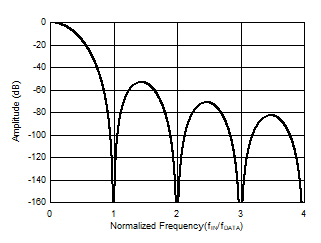
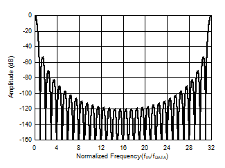
Figure 8-14 and Figure 8-15 show the sinc4 filter frequency response at OSR = 32. The frequency response consists of a series of response nulls occurring at discrete frequencies. The null frequencies occur at multiples of fDATA. At the null frequencies, the filter has zero gain. A folded image of the overall frequency response appears at multiples of fMOD, as illustrated in the fMOD frequency plot of Figure 8-15. No attenuation is provided by the filter at input frequencies near n · fMOD (n = 1, 2, 3, and so on), and if present, alias into the pass band.
 Figure 8-14 Sinc4 Frequency
Response
Figure 8-14 Sinc4 Frequency
Response(OSR = 32)
 Figure 8-15 Sinc4 Frequency Response
to fMOD (OSR = 32)