ZHCSES2H December 2009 – February 2016 ADS1282-HT
PRODUCTION DATA.
- 1 特性
- 2 应用
- 3 说明
- 4 修订历史记录
- 5 说明 (续)
- 6 Pin Configuration and Functions
-
7 Specifications
- 7.1 Absolute Maximum Ratings
- 7.2 Recommended Operating Conditions
- 7.3 Thermal Information
- 7.4 Electrical Characteristics
- 7.5 Electrical Characteristics (PW Package)
- 7.6 Timing Requirements
- 7.7 Pulse-Sync Timing Requirements
- 7.8 Reset Timing Requirements
- 7.9 Switching Characteristics
- 7.10 Modulator Switching Characteristics
- 7.11 Typical Characteristics
-
8 Detailed Description
- 8.1 Overview
- 8.2 Functional Block Diagram
- 8.3
Feature Description
- 8.3.1 Noise Performance
- 8.3.2 Input-Referred Noise
- 8.3.3 Idle Tones
- 8.3.4 Operating Mode
- 8.3.5 Analog Inputs and Multiplexer
- 8.3.6 PGA (Programmable Gain Amplifier)
- 8.3.7 ADC
- 8.3.8 Modulator
- 8.3.9 Modulator Over-Range
- 8.3.10 Modulator Input Impedance
- 8.3.11 Modulator Over-Range Detection (MFLAG)
- 8.3.12 Voltage Reference Inputs (VREFP, VREFN)
- 8.3.13 Digital Filter
- 8.3.14 Master Clock Input (CLK)
- 8.3.15 Synchronization (SYNC Pin and Sync Command)
- 8.3.16 Pulse-Sync Mode
- 8.3.17 Continuous-Sync Mode
- 8.3.18 Reset (RESET Pin and Reset Command)
- 8.3.19 Power-Down (PWDN Pin and Standby Command)
- 8.3.20 Power-On Sequence
- 8.3.21 Serial Interface
- 8.3.22 Data Format
- 8.3.23 Reading Data
- 8.3.24 One-Shot Operation
- 8.4 Device Functional Modes
- 8.5
Programming
- 8.5.1
Commands
- 8.5.1.1 WAKEUP: Wake-Up from Standby Mode
- 8.5.1.2 STANDBY: Standby Mode
- 8.5.1.3 SYNC: Synchronize the A/D Conversion
- 8.5.1.4 RESET: Reset the Device
- 8.5.1.5 RDATAC: Read Data Continuous
- 8.5.1.6 SDATAC: Stop Read Data Continuous
- 8.5.1.7 RDATA: Read Data By Command
- 8.5.1.8 RREG: Read Register Data
- 8.5.1.9 WREG: Write to Register
- 8.5.1.10 OFSCAL: Offset Calibration
- 8.5.1.11 GANCAL: Gain Calibration
- 8.5.2 Calibration Commands
- 8.5.3 User Calibration
- 8.5.4 Configuration Guide
- 8.5.1
Commands
- 8.6 Register Maps
- 9 Application and Implementation
- 10Power Supply Recommendations
- 11器件和文档支持
- 12机械、封装和可订购信息
封装选项
机械数据 (封装 | 引脚)
散热焊盘机械数据 (封装 | 引脚)
订购信息
7 Specifications
7.1 Absolute Maximum Ratings
over operating free-air temperature (unless otherwise noted)(1)| MIN | MAX | UNIT | ||
|---|---|---|---|---|
| AVDD to AVSS | –0.3 | 5.5 | V | |
| AVSS to DGND | –2.8 | 0.3 | V | |
| DVDD to DGND | –0.3 | 3.9 | V | |
| Input current | 100, momentary | mA | ||
| Input current | 10, continuous | mA | ||
| Analog input voltage (AINP1, AINN1, AINP2, AINN2, VREFN, VREFP, CAPP, CAPN) | AVSS – 0.3 | AVDD + 0.3 | V | |
| Digital input voltage to DGND (CLK, SCLK, DRDY, DOUT, DIN, MCLK, M1, M0, MFLAG, SYNC, PWDN, RESET) | –0.3 | DVDD + 0.3 | V | |
| Storage temperature, Tstg | –60 | 150 | °C | |
(1) Stresses beyond those listed under Absolute Maximum Ratings may cause permanent damage to the device. These are stress ratings only, which do not imply functional operation of the device at these or any other conditions beyond those indicated under Recommended Operating Conditions. Exposure to absolute-maximum-rated conditions for extended periods may affect device reliability.
7.2 Recommended Operating Conditions
over operating free-air temperature range (unless otherwise noted)| MIN | NOM | MAX | UNIT | ||
|---|---|---|---|---|---|
| Operating temperature | –55 | 125 | °C | ||
7.3 Thermal Information
| THERMAL METRIC(1) | ADS1282-HT | UNIT | ||
|---|---|---|---|---|
| JDJ (CDIP SB) | PW (TSSOP) | |||
| 28 PINS | 28 PINS | |||
| RθJA | Junction-to-ambient thermal resistance | 43.1 | 54.6 | °C/W |
| RθJC(top) | Junction-to-case (top) thermal resistance | 14.03 | 11.3 | °C/W |
| RθJB | Junction-to-board thermal resistance | 23.2 | 13 | °C/W |
| ψJT | Junction-to-top characterization parameter | N/A | 0.5 | °C/W |
| ψJB | Junction-to-board characterization parameter | N/A | 12.7 | °C/W |
| RθJC(bot) | Junction-to-case (bottom) thermal resistance | 4.98 | N/A | °C/W |
(1) For more information about traditional and new thermal metrics, see the Semiconductor and IC Package Thermal Metrics application report, SPRA953.
7.4 Electrical Characteristics
Limit specifications at –55°C to 210°C. Typical specifications at 25°C, AVDD = 2.5 V, AVSS = –2.5 V, ƒCLK(1) = 4.096 MHz, VREFP = 2.5 V, VREFN = –2.5 V, DVDD = 3.3 V, CAPN – CAPP = 10 nF, PGA = 1, and ƒDATA = 1000 SPS, unless otherwise noted.| PARAMETER | TEST CONDITIONS | TA = –55°C to 125°C | TA = 210°C(2) | UNIT | |||||
|---|---|---|---|---|---|---|---|---|---|
| MIN | TYP | MAX | MIN | TYP | MAX | ||||
| ANALOG INPUTS | |||||||||
| Full-scale input voltage | VIN = (AINP – AINN) | ±VREF/(2 × PGA) | V | ||||||
| Absolute input range | AINP or AINN |
AVSS + 0.7 | AVDD – 1.25 | AVSS + 0.7 | AVDD – 1.25 | V | |||
| PGA input voltage noise density | 5 | nV/√Hz | |||||||
| Differential input impedance(3) | 1 | GΩ | |||||||
| Common-mode input impedance | 100 | MΩ | |||||||
| Input bias current | 1 | 1000 | nA | ||||||
| Crosstalk | ƒ = 31.25 Hz | –128 | –123 | dB | |||||
| MUX ON-resistance | 30 | 45 | Ω | ||||||
| PGA OUTPUT (CAPP, CAPN) | |||||||||
| Absolute output range | AVSS + 0.4 | AVDD – 0.4 | AVSS + 0.4 | AVDD – 0.4 | V | ||||
| PGA differential output impedance | 600 | 600 | Ω | ||||||
| Output impedance tolerance | ±10% | ±10% | |||||||
| External bypass capacitance | 10 | 100 | 10 | nF | |||||
| Modulator differential input impedance | 55 | kΩ | |||||||
| AC PERFORMANCE | |||||||||
| Signal-to-noise ratio(4) | SNR | 112 | 124 | 110 | 122 | dB | |||
| Total harmonic distortion(5) | THD | PGA = 1...16 | –122 | –99 | –102 | –99 | dB | ||
| PGA = 32 | –117 | –99 | –98 | –94 | |||||
| PGA = 64 | –115 | –93 | |||||||
| Spurious-free dynamic range | SFDR | 123 | dB | ||||||
| DC PERFORMANCE | |||||||||
| Resolution | No missing codes | 31 | 31 | bits | |||||
| Data rate | ƒDATA | FIR filter mode | 250 | 4000 | 250 | 4000 | SPS | ||
| Sinc filter mode | 8000 | 128000 | 8000 | 128000 | SPS | ||||
| Integral nonlinearity (INL)(6) | Differential input | 0.00005 | 0.0090 | 0.002 | 0.01 | % FSR(7) | |||
| Offset error | Shorted input | 50 | 200 | 99 | 250 | μV | |||
| Offset error after calibration(8) | 1 | 2 | μV | ||||||
| Offset drift | 0.02 | 0.19 | μV/°C | ||||||
| Gain error(9) | –1.5% | –1% | –0.5% | –1.5% | –1% | –0.5% | |||
| Gain error after calibration(8) | 0.0002% | 0.0002% | |||||||
| Gain drift | PGA = 1 | 2 | 3 | ppm/°C | |||||
| PGA = 16 | 9 | 11 | ppm/°C | ||||||
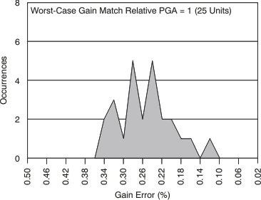
| Gain matching(13) | 0.3% | 0.8% | 0.8% | ||||||
| Common-mode rejection | ƒCM = 60 Hz(10) | 82 | 110 | 82 | 137 | dB | |||
| Power-supply rejection | AVDD, AVSS | ƒPS = 60 Hz(10) | 80 | 90 | 83 | dB | |||
| DVDD | 90 | 115 | 101 | ||||||
| VOLTAGE REFERENCE INPUTS | |||||||||
| Reference input voltage | (VREF = VREFP – VREFN) | 0.5 | 5 | (AVDD – AVSS) + 0.2 | 0.5 | (AVDD – AVSS) + 0.2 | V | ||
| Negative reference input | VREFN | AVSS – 0.1 | VREFP – 0.5 | AVSS – 0.1 | VREFP – 0.5 | V | |||
| Positive reference input | VREFP | VREFN + 0.5 | AVDD + 0.1 | VREFN + 0.5 | AVDD + 0.1 | V | |||
| Reference input impedance | 85 | 85 | kΩ | ||||||
| DIGITAL FILTER RESPONSE | |||||||||
| Passband ripple | ±0.003 | dB | |||||||
| Passband (–0.01 dB) | 0.375 × ƒDATA | Hz | |||||||
| Bandwidth (–3 dB) | 0.413 × ƒDATA | Hz | |||||||
| High-pass filter corner | 0.1 | 10 | Hz | ||||||
| Stop band attenuation(11) | 135 | dB | |||||||
| Stop band | 0.500 × ƒDATA | Hz | |||||||
| Group delay | Minimum phase filter | 5 / ƒDATA | s | ||||||
| Linear phase filter | 31 / ƒDATA | ||||||||
| Settling time (latency) | Minimum phase filter | 62 / ƒDATA | s | ||||||
| Linear phase filter | 62 / ƒDATA | s | |||||||
| DIGITAL INPUT/OUTPUT | |||||||||
| VIH | 0.8 × DVDD | DVDD | 0.8 × DVDD | DVDD | V | ||||
| VIL | DGND | 0.2 × DVDD | DGND | 0.2 × DVDD | V | ||||
| VOH | IOH = 1 mA | 0.8 × DVDD | 0.8 × DVDD | V | |||||
| VOL | IOL = 1 mA | 0.2 × DVDD | 0.2 × DVDD | V | |||||
| Input leakage | 0 < VDIGITAL IN < DVDD | ±10 | ±10 | μA | |||||
| POWER SUPPLY | |||||||||
| AVSS | –2.6 | 0 | –2.6 | 0 | V | ||||
| AVDD | AVSS + 4.75 | AVSS + 5.25 | AVSS + 4.75 | AVSS + 5.25 | V | ||||
| DVDD | 1.75 | 3.6 | 1.75 | 3.6 | V | ||||
| AVDD, AVSS current | High-resolution mode | 4.5 | 7.2 | 5.2 | 10 | |mA| | |||
| Standby mode | 68 | 250 | 3000 | 3700 | |μA| | ||||
| Power-down mode | 68 | 250 | 3000 | 3700 | |μA| | ||||
| DVDD current | All modes | 0.6 | 1.5 | 1.2 | 2 | mA | |||
| Modulator mode | 0.1 | 1.1 | mA | ||||||
| Standby mode | 73 | 175 | 576 | 950 | μA | ||||
| Power-down mode(12) | 32 | 120 | 186 | 240 | μA | ||||
| Power dissipation | High-resolution mode | 25 | 41 | 29.7 | 56.1 | mW | |||
| Standby mode | 0.58 | 1.1 | 16.9 | 21.6 | mW | ||||
| Power-down mode | 0.45 | 0.95 | 15.6 | 19.3 | mW | ||||
(1) ƒCLK = system clock.
(2) Minimum and maximum parameters are characterized for operation at TA = 210°C, but may not be production tested at that temperature. Production test limits with statistical guardbands are used to ensure high temperature performance.
(3) Input impedance is improved by disabling input chopping (CHOP bit = 0).
(4) VIN = 20mVDC/PGA, see Table 1.
(5) VIN = 31.25 Hz, –0.5 dBFS.
(6) Best-fit method.
(7) FSR: Full-scale range = ±VREF / (2 × PGA).
(8) Calibration accuracy is on the level of noise reduced by 4 (calibration averages 16 readings).
(9) The PGA output impedance and the modulator input impedance results in –1% systematic gain error.
(10) ƒCM is the input common-mode frequency. ƒPS is the power-supply frequency.
(11) Input frequencies in the range of NƒCLK / 512 ± ƒDATA / 2 (N = 1, 2, 3...) can mix with the modulator chopping clock. In these frequency ranges intermodulation = 120 dB, typ.
(12) CLK input stopped.
(13) Gain match relative to PGA = 1.
7.5 Electrical Characteristics (PW Package)
Limit specifications at –55°C to 175°C. Typical specifications at 25°C, AVDD = 2.5 V, AVSS = –2.5 V, ƒCLK(1) = 4.096 MHz, VREFP = 2.5 V, VREFN = –2.5 V, DVDD = 3.3 V, CAPN – CAPP = 10 nF, PGA = 1, and ƒDATA = 1000 SPS, unless otherwise noted.| PARAMETER | TEST CONDITIONS | TA = –55°C to 125°C | TA = 175°C(2) | UNIT | |||||
|---|---|---|---|---|---|---|---|---|---|
| MIN | TYP | MAX | MIN | TYP | MAX | ||||
| ANALOG INPUTS | |||||||||
| Full-scale input voltage | VIN = (AINP – AINN) | ±VREF / (2 × PGA) | ±VREF / (2 × PGA) | V | |||||
| Absolute input range | AINP or AINN |
AVSS + 0.7 | AVDD – 1.25 | AVSS + 0.7 | AVDD – 1.25 | V | |||
| PGA input voltage noise density | 5 | 5 | nV/√Hz | ||||||
| Differential input impedance(3) | 1 | 1 | GΩ | ||||||
| Common-mode input impedance | 100 | 100 | MΩ | ||||||
| Input bias current | 1 | 1000 | nA | ||||||
| Crosstalk | f = 31.25 Hz | –128 | –123 | dB | |||||
| MUX on-resistance | 30 | 45 | Ω | ||||||
| PGA OUTPUT (CAPP, CAPN) | |||||||||
| Absolute output range | AVSS + 0.4 | AVDD – 0.4 | AVSS + 0.4 | AVDD – 0.4 | V | ||||
| PGA differential output impedance | 600 | 600 | Ω | ||||||
| Output impedance tolerance | ±10% | ±10% | |||||||
| External bypass capacitance | 10 | 100 | 10 | nF | |||||
| Modulator differential input impedance | 55 | 55 | kΩ | ||||||
| AC PERFORMANCE | |||||||||
| Signal-to-noise ratio(4) | SNR | 112 | 124 | 112 | 122 | dB | |||
| Total harmonic distortion(5) | THD | PGA = 1...16 | –122 | –99 | –112 | –99 | dB | ||
| PGA = 32 | –117 | –99 | –106 | –94 | |||||
| PGA = 64 | –115 | –102 | |||||||
| Spurious-free dynamic range | SFDR | 123 | dB | ||||||
| DC PERFORMANCE | |||||||||
| Resolution | No missing codes | 31 | 31 | bits | |||||
| Data rate | ƒDATA | FIR filter mode | 250 | 4000 | 250 | 4000 | SPS | ||
| Sinc filter mode | 8000 | 128000 | 8000 | 128000 | SPS | ||||
| Integral nonlinearity (INL)(6) | Differential input | 0.00005 | 0.009 | 0.00004 | 0.009 | % FSR(7) | |||
| Offset error | Shorted input | 50 | 200 | 50 | 200 | μV | |||
| Offset error after calibration(8) | 1 | 2 | μV | ||||||
| Offset drift | 0.02 | 0.19 | μV/°C | ||||||
| Gain error(9) | –1.5% | –1% | –0.5% | –1.5% | –1% | –0.5% | |||
| Gain error after calibration(8) | 0.0002% | 0.0002% | |||||||
| Gain drift | PGA = 1 | 2 | 2 | ppm/°C | |||||
| PGA = 16 | 9 | 11 | ppm/°C | ||||||
| Gain matching(13) | 0.3% | 0.8% | 0.4% | 0.8% | |||||
| Common-mode rejection | ƒCM = 60 Hz(10) | 82 | 110 | 82 | 114 | dB | |||
| Power-supply rejection | AVDD, AVSS | ƒPS = 60 Hz(10) | 80 | 90 | 84 | dB | |||
| DVDD | 90 | 115 | 106 | ||||||
| VOLTAGE REFERENCE INPUTS | |||||||||
| Reference input voltage | (VREF = VREFP – VREFN) | 0.5 | 5 | (AVDD – AVSS) + 0.2 | 0.5 | (AVDD – AVSS) + 0.2 | V | ||
| Negative reference input | VREFN | AVSS – 0.1 | VREFP – 0.5 | AVSS – 0.1 | VREFP – 0.5 | V | |||
| Positive reference input | VREFP | VREFN + 0.5 | AVDD + 0.1 | VREFN + 0.5 | AVDD + 0.1 | V | |||
| Reference input impedance | 85 | 85 | kΩ | ||||||
| DIGITAL FILTER RESPONSE | |||||||||
| Passband ripple | ±0.003 | ±0.003 | dB | ||||||
| Passband (–0.01 dB) | 0.375 × ƒDATA | 0.375 × ƒDATA | Hz | ||||||
| Bandwidth (–3 dB) | 0.413 × ƒDATA | 0.413 × ƒDATA | Hz | ||||||
| High-pass filter corner | 0.1 | 10 | 0.1 | 10 | Hz | ||||
| Stop band attenuation(11) | 135 | 135 | dB | ||||||
| Stop band | 0.500 × ƒDATA | 0.500 × ƒDATA | Hz | ||||||
| DIGITAL INPUT/OUTPUT | |||||||||
| VIH | 0.8 × DVDD | DVDD | 0.8 × DVDD | DVDD | V | ||||
| VIL | DGND | 0.2 × DVDD | DGND | 0.2 × DVDD | V | ||||
| VOH | IOH = 1 mA | 0.8 × DVDD | 0.8 × DVDD | V | |||||
| VOL | IOL = 1 mA | 0.2 × DVDD | 0.2 × DVDD | V | |||||
| Input leakage | 0 < VDIGITAL IN < DVDD | ±10 | ±10 | μA | |||||
| POWER SUPPLY | |||||||||
| AVSS | –2.6 | 0 | –2.6 | 0 | V | ||||
| AVDD | AVSS + 4.75 | AVSS + 5.25 | AVSS + 4.75 | AVSS + 5.25 | V | ||||
| DVDD | 1.75 | 3.6 | 1.75 | 3.6 | V | ||||
| AVDD, AVSS current | High-resolution mode | 4.5 | 7.2 | 5.2 | 9.2 | |mA| | |||
| Standby mode | 68 | 110 | 52 | 900 | |μA| | ||||
| Power-down mode | 68 | 110 | 52 | 900 | |μA| | ||||
| DVDD current | All modes | 0.6 | 1.5 | 0.7 | 1.5 | mA | |||
| Modulator mode | 0.1 | 1.05 | mA | ||||||
| Standby mode | 73 | 175 | 255 | 600 | μA | ||||
| Power-down mode(12) | 32 | 120 | 118 | 220 | μA | ||||
| Power dissipation | High-resolution mode | 25 | 41 | 31 | 41 | mW | |||
| Standby mode | 0.58 | 1.1 | 2.5 | 5 | mW | ||||
| Power-down mode | 0.45 | 0.95 | 2.06 | 4.5 | mW | ||||
(1) ƒCLK = System clock
(2) Minimum and maximum parameters are characterized for operation at TA = 175°C, but may not be production tested at that temperature. Production test limits with statistical guardbands are used to ensure high temperature performance.
(3) Input impedance is improved by disabling input chopping (CHOP bit = 0).
(4) VIN = 20 mVDC / PGA, see Table 1.
(5) VIN = 31.25 Hz, –0.5 dBFS.
(6) Best-fit method.
(7) FSR: Full-scale range = ±VREF / (2 × PGA).
(8) Calibration accuracy is on the level of noise reduced by 4 (calibration averages 16 readings).
(9) The PGA output impedance and the modulator input impedance results in –1% systematic gain error.
(10) ƒCM is the input common-mode frequency. ƒPS is the power-supply frequency.
(11) Input frequencies in the range of NƒCLK / 512 ± ƒDATA / 2 (N = 1, 2, 3...) can mix with the modulator chopping clock. In these frequency ranges intermodulation = 120 dB, typ.
(12) CLK input stopped.
(13) Gain match relative to PGA = 1.
7.6 Timing Requirements
At TA = –55°C to 210°C and DVDD = 1.65 to 3.6 V, unless otherwise noted.| TA = –55°C to 125°C | TA = 175°C | TA = 210°C | UNIT | |||||
|---|---|---|---|---|---|---|---|---|
| MIN | MAX | MIN | MAX | MIN | MAX | |||
| tSCLK | SCLK period | 2 | 16 | 2 | 16 | 2 | 16 | 1 / ƒCLK |
| tSPWH, L | SCLK pulse width, high and low(1) | 0.8 | 10 | 0.8 | 10 | 0.8 | 10 | 1 / ƒCLK |
| tDIST | DIN valid to SCLK rising edge: setup time | 50 | 50 | 50 | ns | |||
| tDIHD | Valid DIN to SCLK rising edge: hold time | 50 | 50 | 50 | ns | |||
| tDOPD | SCLK falling edge to valid new DOUT: propagation delay(2) | 100 | 100 | 100 | ns | |||
| tDOHD | SCLK falling edge to DOUT invalid: hold time | 0 | 0 | 0 | ns | |||
| tSCDL | Final SCLK rising edge of command to first SCLK rising edge for register read/write data | 24 | 24 | 24 | 1 / ƒCLK | |||
| DIGITAL INPUT/OUTPUT | ||||||||
| Clock input | ƒCLK | 1 | 4.096 | 1 | 4.096 | MHz | ||
| Serial clock rate | ƒSCLK | ƒCLK/2 | ƒCLK/2 | MHz | ||||
(1) Holding SCLK low for 64 DRDY falling edges resets the serial interface.
(2) Load on DOUT = 20 pF || 100 kΩ.
7.7 Pulse-Sync Timing Requirements
See Figure 46 and Figure 47 for timing diagrams.| MIN | MAX | UNIT | ||
|---|---|---|---|---|
| tSYNC | SYNC period(1) | 1 | Infinite | n / ƒDATA |
| tCSHD | CLK to SYNC hold time to not latch on CLK edge | 10 | ns | |
| tSCSU | SYNC to CLK setup time to latch on CLK edge | 10 | ns | |
| tSPWH, L | SYNC pulse width, high or low | 2 | 1 / ƒCLK | |
| tDR | Time for data ready (SINC filter) | See 器件支持, Table 20 | ||
| Time for data ready (FIR filter) | 62.98046875 / ƒDATA + 466 / ƒCLK | |||
(1) Continuous-Sync mode; a free-running SYNC clock input without causing re-synchronization.
7.8 Reset Timing Requirements
See Figure 48 for timing diagram.| MIN | MAX | UNIT | ||
|---|---|---|---|---|
| tCRHD | CLK to RESET hold time | 10 | ns | |
| tRCSU | RESET to CLK setup time | 10 | ns | |
| tRST | RESET low | 2 | 1 / ƒCLK | |
| tDR | Time for data ready | 62.98046875 / ƒDATA + 468 / ƒCLK | s | |
Read Data Timing Requirements
| MIN | MAX | UNIT | ||
|---|---|---|---|---|
| tDDPD | DRDY to valid MSB on DOUT propagation delay (see Figure 54)(1) | 100 | ns | |
| tDR | Time for new data after data read command (see Figure 55) | 0 | 1 | ƒDATA |
(1) Load on DOUT = 20 pF || 100 kΩ.
7.9 Switching Characteristics
over operating free-air temperature range (unless otherwise noted)| PARAMETER | TEST CONDITIONS | MIN | TYP | MAX | UNIT | |
|---|---|---|---|---|---|---|
| Group delay(1) | Minimum phase filter | 5 / ƒDATA | s | |||
| Linear phase filter | 31 / ƒDATA | s | ||||
| Settling time (latency) | Minimum phase filter | 62 / ƒDATA | s | |||
| Linear phase filter | 62 / ƒDATA | s | ||||
(1) At DC. See Figure 42.
7.10 Modulator Switching Characteristics
See Figure 56.| PARAMETER | TEST CONDITIONS | MIN | TYP | MAX | UNIT | ||
|---|---|---|---|---|---|---|---|
| tMCD0, 1 | MCLK rising edge to M0, M1 valid propagation delay(1) | 100 | ns | ||||
| tCMD | CLK rising edge (after SYNC rising edge) to MCLK rising edge CMD | 5 | 1/ƒCLK | ||||
| tCSHD | CLK to SYNC hold time to not latch on CLK edge | 10 | ns | ||||
| tSCSU | SYNC to CLK setup time to latch on CLK edge | 10 | ns | ||||
| tSYMD | SYNC to stable bit stream | 16 | 1/ƒMOD | ||||
(1) Load on M0 and M1 = 20 pF || 100 kΩ.
 Figure 1. Timing Diagram
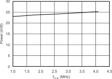
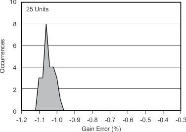
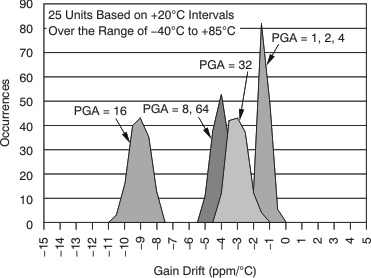
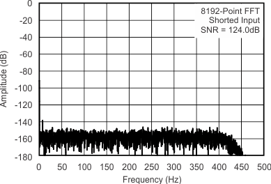
7.11 Typical Characteristics
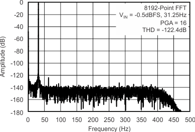
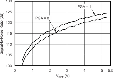
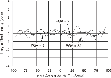
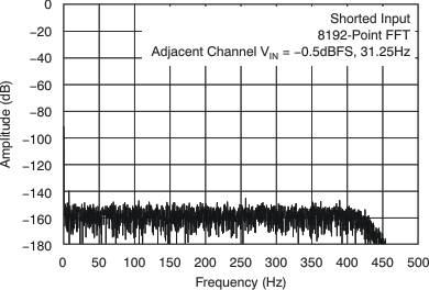
At 25°C, AVDD = 2.5 V, AVSS = –2.5 V, ƒCLK = 4.096 MHz, VREFP = 2.5 V, VREFN = –2.5 V, DVDD = 3.3 V, CAPN – CAPP = 10 nF, PGA = 1, and ƒDATA = 1000 SPS, unless otherwise noted.