ZHCSES1B March 2016 – October 2018 ADS1282-SP
PRODUCTION DATA.
- 1 特性
- 2 应用
- 3 说明
- 4 修订历史记录
- 5 (说明 (续))
- 6 Pin Configuration and Functions
-
7 Specifications
- 7.1 Absolute Maximum Ratings
- 7.2 ESD Ratings
- 7.3 Recommended Operating Conditions
- 7.4 Thermal Information
- 7.5 Electrical Characteristics
- 7.6 Timing Requirements
- 7.7 Pulse-Sync Timing Requirements
- 7.8 Reset Timing Requirements
- 7.9 Read Data Timing Requirements
- 7.10 Switching Characteristics
- 7.11 Typical Characteristics
-
8 Detailed Description
- 8.1 Overview
- 8.2 Functional Block Diagram
- 8.3
Feature Description
- 8.3.1 Noise Performance
- 8.3.2 Input-Referred Noise
- 8.3.3 Idle Tones
- 8.3.4 Operating Mode
- 8.3.5 Analog Inputs and Multiplexer
- 8.3.6 PGA (Programmable Gain Amplifier)
- 8.3.7 ADC
- 8.3.8 Modulator
- 8.3.9 Modulator Over-Range
- 8.3.10 Modulator Input Impedance
- 8.3.11 Modulator Over-Range Detection (MFLAG)
- 8.3.12 Voltage Reference Inputs (VREFP, VREFN)
- 8.3.13 Digital Filter
- 8.3.14 Master Clock Input (CLK)
- 8.3.15 Synchronization (SYNC Pin and Sync Command)
- 8.3.16 Pulse-Sync Mode
- 8.3.17 Continuous-Sync Mode
- 8.3.18 Reset (RESET Pin and Reset Command)
- 8.3.19 Power-Down (PWDN Pin and Standby Command)
- 8.3.20 Power-On Sequence
- 8.3.21 Serial Interface
- 8.3.22 Data Format
- 8.3.23 Reading Data
- 8.3.24 One-Shot Operation
- 8.4 Device Functional Modes
- 8.5
Programming
- 8.5.1
Commands
- 8.5.1.1 WAKEUP: Wake-Up from Standby Mode
- 8.5.1.2 STANDBY: Standby Mode
- 8.5.1.3 SYNC: Synchronize the A/D Conversion
- 8.5.1.4 RESET: Reset the Device
- 8.5.1.5 RDATAC: Read Data Continuous
- 8.5.1.6 SDATAC: Stop Read Data Continuous
- 8.5.1.7 RDATA: Read Data By Command
- 8.5.1.8 RREG: Read Register Data
- 8.5.1.9 WREG: Write to Register
- 8.5.1.10 OFSCAL: Offset Calibration
- 8.5.1.11 GANCAL: Gain Calibration
- 8.5.2 Calibration Commands
- 8.5.3 User Calibration
- 8.5.4 Configuration Guide
- 8.5.1
Commands
- 8.6 Register Maps
- 9 Application and Implementation
- 10Power Supply Recommendations
- 11Layout
- 12器件和文档支持
- 13机械、封装和可订购信息
9.2.1.1 Design Requirements
Since the output voltages of common thermocouple types are well documented, the accuracy of a thermocouple measurement reduces to accurately measuring the output voltage of the thermocouple at the cold junction and accurately determining the temperature at that cold junction. Once the cold junction temperature is determined, the output voltage can be compensated to reflect the actual hot junction temperature. This compensation can be implemented in hardware on the analog front-end or in software and/or firmware on the digital back-end, each of which presents its own challenges. Analog compensation is challenging in that any components used in compensation circuits are also potential sources of error while back-end digital compensation puts additional processing requirements and algorithms on the FPGA or microprocessor. The premise of this application writing is that cold junction compensation will be implemented in the digital domain so that minimal circuitry is used in the analog domain. With this, the front-end design goal becomes effectively digitizing the thermocouple output voltage as well as the cold junction temperature voltage.
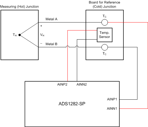
The ADS1282-SP is ideal for achieving these goals as the device offers two analog inputs that are mux’d to one delta-sigma modulator. Figure 77 illustrates how one input receives the thermocouple output voltage while the second receives the cold junction compensation voltage. The Temp Sensor shown in the figure can take on many forms such as a temp sensor IC, an RTD, or a thermistor.
 Figure 77. ADS1282-SP as Thermocouple DAQ
 The ADS1282-SP offers a very high dynamic range. To realize this dynamic range, however, the small thermocouple voltage requires amplification to make use of the full scale range (FSR) of the ADC. The integrated programmable gain amplifier (PGA) provides this amplification in factors of 1x to 64x (in powers of 2) making the ADS1282-SP versatile for use with different types of thermocouples.
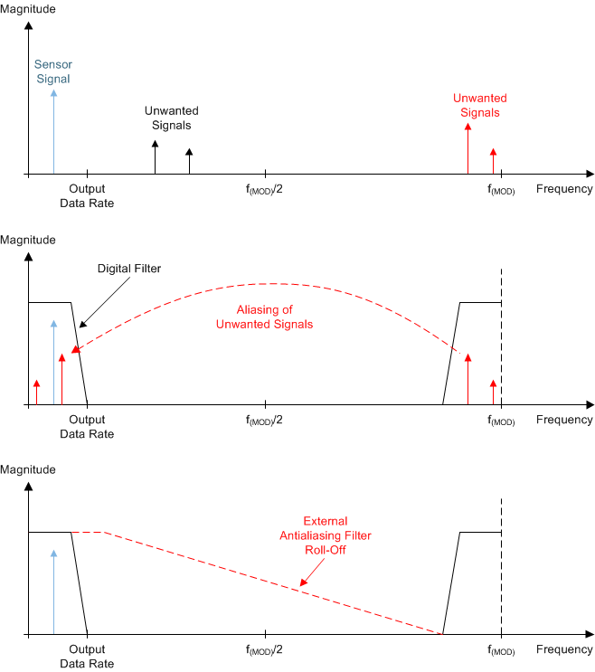
In addition to amplification, the analog input should be filtered. Filtering serves two purposes: first, to limit the effect of aliasing during the sampling process and second, to reduce external noise from becoming a part of the measurement. As with any sampled system, aliasing can occur if proper anti-alias filtering is not in place. Aliasing occurs when frequency components are present in the input signal that are higher than half the sampling frequency of the ADC (also known as the Nyquist frequency). These frequency components fold back and show up in the actual frequency band of interest below half the sampling frequency. The filter response of the digital filter repeats at multiples of the sampling frequency, also known as modulator frequency f(MOD), as shown in Figure 78. Any frequency components present in the input signal around the modulator frequency or multiples thereof are not attenuated and alias back into the band of interest, unless attenuated by an external analog filter.
 Figure 78. Effect of Aliasing
 Many sensor signals, such as the thermocouple, are inherently band-limited; the output has a limited rate of change. In this case, the sensor signal does not alias back into the pass-band when using a ΔΣ ADC. However, any noise pickup along the sensor wiring or the application circuitry can potentially alias into the pass band. Power line-cycle frequency and harmonics are one common noise source. External noise can also be generated from electromagnetic interference (EMI) or radio frequency interference (RFI) sources, such as nearby motors and RF transceivers. Another noise source typically exists on the printed-circuit-board (PCB) itself in the form of clocks and other digital signals. Analog input filtering helps remove unwanted signals from affecting the measurement result. A first-order, resistor-capacitor (RC) filter is, in most cases, sufficient to either eliminate such noise, or to reduce the effects to a level within the noise floor of the sensor.