ZHCSES1B March 2016 – October 2018 ADS1282-SP
PRODUCTION DATA.
- 1 特性
- 2 应用
- 3 说明
- 4 修订历史记录
- 5 (说明 (续))
- 6 Pin Configuration and Functions
-
7 Specifications
- 7.1 Absolute Maximum Ratings
- 7.2 ESD Ratings
- 7.3 Recommended Operating Conditions
- 7.4 Thermal Information
- 7.5 Electrical Characteristics
- 7.6 Timing Requirements
- 7.7 Pulse-Sync Timing Requirements
- 7.8 Reset Timing Requirements
- 7.9 Read Data Timing Requirements
- 7.10 Switching Characteristics
- 7.11 Typical Characteristics
-
8 Detailed Description
- 8.1 Overview
- 8.2 Functional Block Diagram
- 8.3
Feature Description
- 8.3.1 Noise Performance
- 8.3.2 Input-Referred Noise
- 8.3.3 Idle Tones
- 8.3.4 Operating Mode
- 8.3.5 Analog Inputs and Multiplexer
- 8.3.6 PGA (Programmable Gain Amplifier)
- 8.3.7 ADC
- 8.3.8 Modulator
- 8.3.9 Modulator Over-Range
- 8.3.10 Modulator Input Impedance
- 8.3.11 Modulator Over-Range Detection (MFLAG)
- 8.3.12 Voltage Reference Inputs (VREFP, VREFN)
- 8.3.13 Digital Filter
- 8.3.14 Master Clock Input (CLK)
- 8.3.15 Synchronization (SYNC Pin and Sync Command)
- 8.3.16 Pulse-Sync Mode
- 8.3.17 Continuous-Sync Mode
- 8.3.18 Reset (RESET Pin and Reset Command)
- 8.3.19 Power-Down (PWDN Pin and Standby Command)
- 8.3.20 Power-On Sequence
- 8.3.21 Serial Interface
- 8.3.22 Data Format
- 8.3.23 Reading Data
- 8.3.24 One-Shot Operation
- 8.4 Device Functional Modes
- 8.5
Programming
- 8.5.1
Commands
- 8.5.1.1 WAKEUP: Wake-Up from Standby Mode
- 8.5.1.2 STANDBY: Standby Mode
- 8.5.1.3 SYNC: Synchronize the A/D Conversion
- 8.5.1.4 RESET: Reset the Device
- 8.5.1.5 RDATAC: Read Data Continuous
- 8.5.1.6 SDATAC: Stop Read Data Continuous
- 8.5.1.7 RDATA: Read Data By Command
- 8.5.1.8 RREG: Read Register Data
- 8.5.1.9 WREG: Write to Register
- 8.5.1.10 OFSCAL: Offset Calibration
- 8.5.1.11 GANCAL: Gain Calibration
- 8.5.2 Calibration Commands
- 8.5.3 User Calibration
- 8.5.4 Configuration Guide
- 8.5.1
Commands
- 8.6 Register Maps
- 9 Application and Implementation
- 10Power Supply Recommendations
- 11Layout
- 12器件和文档支持
- 13机械、封装和可订购信息
8.3.5 Analog Inputs and Multiplexer
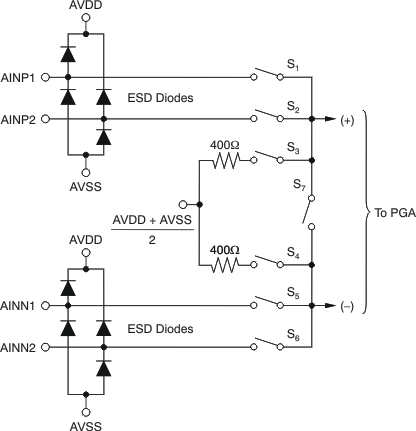
Figure 26 shows a diagram of the input multiplexer.
ESD diodes protect the multiplexer inputs. If either input is taken less than AVSS – 0.3 V or greater than AVDD + 0.3 V, the ESD protection diodes may turn on. If these conditions are possible, external Schottky clamp diodes and/or series resistors may be required to limit the input current to safe values (see the Absolute Maximum Ratings).
Also, overdriving one unused input may affect the conversions of the other input. If overdriven inputs are possible, TI recommends clamping the signal with external Schottky diodes.
 Figure 26. Analog Inputs and Multiplexer
 The specified input operating range of the PGA is shown in Equation 2:
Absolute input levels (input signal level and common-mode level) should be maintained within these limits for best operation.
The multiplexer connects one of the two external differential inputs to the preamplifier inputs, in addition to internal connections for various self-test modes. Table 2 summarizes the multiplexer configurations for Figure 26.
Table 2. Multiplexer Modes
| MUX[2:0] | SWITCHES | DESCRIPTION |
|---|---|---|
| 000 | S1, S5 | AINP1 and AINN1 connected to preamplifier |
| 001 | S2, S6 | AINP2 and AINN2 connected to preamplifier |
| 010 | S3, S4 | Preamplifier inputs shorted together through 400Ω internal resistors |
| 011 | S1, S5, S2, S6 | AINP1, AINN1 and AINP2, AINN2 connected together and to the preamplifier |
| 100 | S6, S7 | External short, preamplifier inputs shorted to AINN2 (common-mode test) |
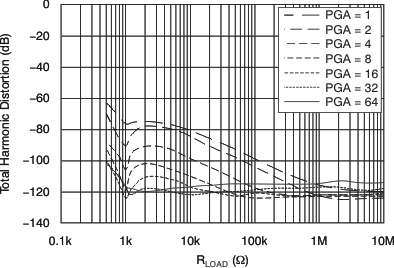
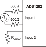
The typical on-resistance (RON) of the multiplexer switch is 30 Ω. When the multiplexer is used to drive an external load on one input by a signal generator on the other input, on-resistance and on-resistance amplitude dependency can lead to measurement errors. Figure 27 shows THD versus load resistance and amplitude. THD improves with high-impedance loads and with lower amplitude drive signals. The data are measured with the circuit from Figure 28 with MUX[2:0] = 011.
 Figure 27. THD vs External Load and Signal Magnitude (PGA) (See Figure 28)
  Figure 28. Driving an External Load Through the MUX