ZHCSES1B March 2016 – October 2018 ADS1282-SP
PRODUCTION DATA.
- 1 特性
- 2 应用
- 3 说明
- 4 修订历史记录
- 5 (说明 (续))
- 6 Pin Configuration and Functions
-
7 Specifications
- 7.1 Absolute Maximum Ratings
- 7.2 ESD Ratings
- 7.3 Recommended Operating Conditions
- 7.4 Thermal Information
- 7.5 Electrical Characteristics
- 7.6 Timing Requirements
- 7.7 Pulse-Sync Timing Requirements
- 7.8 Reset Timing Requirements
- 7.9 Read Data Timing Requirements
- 7.10 Switching Characteristics
- 7.11 Typical Characteristics
-
8 Detailed Description
- 8.1 Overview
- 8.2 Functional Block Diagram
- 8.3
Feature Description
- 8.3.1 Noise Performance
- 8.3.2 Input-Referred Noise
- 8.3.3 Idle Tones
- 8.3.4 Operating Mode
- 8.3.5 Analog Inputs and Multiplexer
- 8.3.6 PGA (Programmable Gain Amplifier)
- 8.3.7 ADC
- 8.3.8 Modulator
- 8.3.9 Modulator Over-Range
- 8.3.10 Modulator Input Impedance
- 8.3.11 Modulator Over-Range Detection (MFLAG)
- 8.3.12 Voltage Reference Inputs (VREFP, VREFN)
- 8.3.13 Digital Filter
- 8.3.14 Master Clock Input (CLK)
- 8.3.15 Synchronization (SYNC Pin and Sync Command)
- 8.3.16 Pulse-Sync Mode
- 8.3.17 Continuous-Sync Mode
- 8.3.18 Reset (RESET Pin and Reset Command)
- 8.3.19 Power-Down (PWDN Pin and Standby Command)
- 8.3.20 Power-On Sequence
- 8.3.21 Serial Interface
- 8.3.22 Data Format
- 8.3.23 Reading Data
- 8.3.24 One-Shot Operation
- 8.4 Device Functional Modes
- 8.5
Programming
- 8.5.1
Commands
- 8.5.1.1 WAKEUP: Wake-Up from Standby Mode
- 8.5.1.2 STANDBY: Standby Mode
- 8.5.1.3 SYNC: Synchronize the A/D Conversion
- 8.5.1.4 RESET: Reset the Device
- 8.5.1.5 RDATAC: Read Data Continuous
- 8.5.1.6 SDATAC: Stop Read Data Continuous
- 8.5.1.7 RDATA: Read Data By Command
- 8.5.1.8 RREG: Read Register Data
- 8.5.1.9 WREG: Write to Register
- 8.5.1.10 OFSCAL: Offset Calibration
- 8.5.1.11 GANCAL: Gain Calibration
- 8.5.2 Calibration Commands
- 8.5.3 User Calibration
- 8.5.4 Configuration Guide
- 8.5.1
Commands
- 8.6 Register Maps
- 9 Application and Implementation
- 10Power Supply Recommendations
- 11Layout
- 12器件和文档支持
- 13机械、封装和可订购信息
8.3.12 Voltage Reference Inputs (VREFP, VREFN)
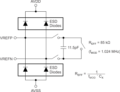
The voltage reference for the ADS1282-SP is the differential voltage between VREFP and VREFN: VREF = VREFP – VREFN. The reference inputs use a structure similar to that of the analog inputs with the circuitry of the reference inputs shown in Figure 35. The average load presented by the switched capacitor reference input can be modeled with an effective differential impedance of REFF = tSAMPLE / CIN (tSAMPLE = 1/ƒMOD). The effective impedance of the reference inputs loads the external reference.
 Figure 35. Simplified Reference Input Circuit
 The ADS1282-SP reference inputs are protected by ESD diodes. In order to prevent these diodes from turning on, the voltage on either input must stay within the range shown in Equation 7:
The minimum valid input for VREFN is AVSS – 0.1 V and maximum valid input for VREFP is AVDD + 0.1 V.
A high-quality 5 V reference voltage is necessary for achieving the best performance from the ADS1282-SP. Noise and drift on the reference degrade overall system performance, and it is critical that special care be given to the circuitry generating the reference voltages in order to achieve full performance. See Application Information for reference recommendations.