ZHCSES1B March 2016 – October 2018 ADS1282-SP
PRODUCTION DATA.
- 1 特性
- 2 应用
- 3 说明
- 4 修订历史记录
- 5 (说明 (续))
- 6 Pin Configuration and Functions
-
7 Specifications
- 7.1 Absolute Maximum Ratings
- 7.2 ESD Ratings
- 7.3 Recommended Operating Conditions
- 7.4 Thermal Information
- 7.5 Electrical Characteristics
- 7.6 Timing Requirements
- 7.7 Pulse-Sync Timing Requirements
- 7.8 Reset Timing Requirements
- 7.9 Read Data Timing Requirements
- 7.10 Switching Characteristics
- 7.11 Typical Characteristics
-
8 Detailed Description
- 8.1 Overview
- 8.2 Functional Block Diagram
- 8.3
Feature Description
- 8.3.1 Noise Performance
- 8.3.2 Input-Referred Noise
- 8.3.3 Idle Tones
- 8.3.4 Operating Mode
- 8.3.5 Analog Inputs and Multiplexer
- 8.3.6 PGA (Programmable Gain Amplifier)
- 8.3.7 ADC
- 8.3.8 Modulator
- 8.3.9 Modulator Over-Range
- 8.3.10 Modulator Input Impedance
- 8.3.11 Modulator Over-Range Detection (MFLAG)
- 8.3.12 Voltage Reference Inputs (VREFP, VREFN)
- 8.3.13 Digital Filter
- 8.3.14 Master Clock Input (CLK)
- 8.3.15 Synchronization (SYNC Pin and Sync Command)
- 8.3.16 Pulse-Sync Mode
- 8.3.17 Continuous-Sync Mode
- 8.3.18 Reset (RESET Pin and Reset Command)
- 8.3.19 Power-Down (PWDN Pin and Standby Command)
- 8.3.20 Power-On Sequence
- 8.3.21 Serial Interface
- 8.3.22 Data Format
- 8.3.23 Reading Data
- 8.3.24 One-Shot Operation
- 8.4 Device Functional Modes
- 8.5
Programming
- 8.5.1
Commands
- 8.5.1.1 WAKEUP: Wake-Up from Standby Mode
- 8.5.1.2 STANDBY: Standby Mode
- 8.5.1.3 SYNC: Synchronize the A/D Conversion
- 8.5.1.4 RESET: Reset the Device
- 8.5.1.5 RDATAC: Read Data Continuous
- 8.5.1.6 SDATAC: Stop Read Data Continuous
- 8.5.1.7 RDATA: Read Data By Command
- 8.5.1.8 RREG: Read Register Data
- 8.5.1.9 WREG: Write to Register
- 8.5.1.10 OFSCAL: Offset Calibration
- 8.5.1.11 GANCAL: Gain Calibration
- 8.5.2 Calibration Commands
- 8.5.3 User Calibration
- 8.5.4 Configuration Guide
- 8.5.1
Commands
- 8.6 Register Maps
- 9 Application and Implementation
- 10Power Supply Recommendations
- 11Layout
- 12器件和文档支持
- 13机械、封装和可订购信息
8.4.1 Modulator Output Mode
The modulator digital stream output is accessible directly, bypassing and disabling the internal digital filter. The modulator output mode is activated by setting the CONFIG0 register bits FILTR[1:0] = 00. Pins M0 and M1 then become the modulator data outputs and the MCLK becomes the modulator clock output. When not in the modulator mode, these pins are inputs and must be tied.
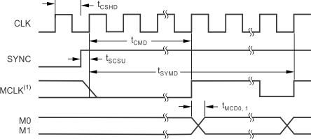
The modulator output is composed of three signals: one output for the modulator clock (MCLK) and two outputs for the modulator data (M0 and M1). The modulator clock output rate is ƒMOD (ƒCLK / 4). The SYNC input resets the MCLK phase, as shown in Figure 56. The SYNC input is latched on the rising edge of CLK. The MCLK resets and the next rising edge of MCLK occurs five CLK periods later.
The modulator output data are two bits wide, which must be merged together before being filtered. Use the time domain equation of Equation 5 to merge the data outputs.

NOINDENT:
MCLK = ƒCLK / 4.Table 10. Modulator Output Timing for Figure 56
| PARAMETER | TEST CONDITIONS | MIN | TYP | MAX | UNIT | ||
|---|---|---|---|---|---|---|---|
| tMCD0, 1 | MCLK rising edge to M0, M1 valid propagation delay | 100 | ns | ||||
| tCMD | CLK rising edge (after SYNC rising edge) to MCLK rising edge CMD | 5 | 1/ƒCLK | ||||
| tCSHD | CLK to SYNC hold time to not latch on CLK edge | 10 | ns | ||||
| tSCSU | SYNC to CLK setup time to latch on CLK edge | 10 | ns | ||||
| tSYMD | SYNC to stable bit stream | 16 | 1/ƒMOD | ||||