ZHCSIU4A September 2018 – August 2019 ADS1284
PRODUCTION DATA.
- 1 特性
- 2 应用
- 3 说明
- 4 修订历史记录
- 5 Pin Configuration and Functions
- 6 Specifications
- 7 Parameter Measurement Information
-
8 Detailed Description
- 8.1 Overview
- 8.2 Functional Block Diagram
- 8.3 Feature Description
- 8.4
Device Functional Modes
- 8.4.1 Synchronization (SYNC PIN and SYNC Command)
- 8.4.2 Reset (RESET Pin and Reset Command)
- 8.4.3 Master Clock Input (CLK)
- 8.4.4 Power-Down (PWDN Pin and STANDBY Command)
- 8.4.5 Power-On Sequence
- 8.4.6 DVDD Power Supply
- 8.4.7 Serial Interface
- 8.4.8 Data Format
- 8.4.9 Reading Data
- 8.4.10 One-Shot Operation
- 8.4.11 Offset and Full-Scale Calibration Registers
- 8.4.12 Calibration Commands (OFSCAL and GANCAL)
- 8.4.13 User Calibration
- 8.5
Programming
- 8.5.1
Commands
- 8.5.1.1 SDATAC Requirements
- 8.5.1.2 WAKEUP: Wake-Up From Standby Mode
- 8.5.1.3 STANDBY: Standby Mode
- 8.5.1.4 SYNC: Synchronize the Analog-to-Digital Conversion
- 8.5.1.5 RESET: Reset the Device
- 8.5.1.6 RDATAC: Read Data Continuous
- 8.5.1.7 SDATAC: Stop Read Data Continuous
- 8.5.1.8 RDATA: Read Data by Command
- 8.5.1.9 RREG: Read Register Data
- 8.5.1.10 WREG: Write to Register
- 8.5.1.11 OFSCAL: Offset Calibration
- 8.5.1.12 GANCAL: Gain Calibration
- 8.5.1
Commands
- 8.6
Register Maps
- 8.6.1
Register Descriptions
- 8.6.1.1 ID_CFG: ID_Configuration Register (address = 00h) [reset =x0h]
- 8.6.1.2 CONFIG0: Configuration Register 0 (address = 01h) [reset = 52h]
- 8.6.1.3 CONFIG1: Configuration Register 1 (address = 02h) [reset = 08h]
- 8.6.1.4 HPF0 and HPF1 Registers
- 8.6.1.5 OFC0, OFC1, OFC2 Registers
- 8.6.1.6 FSC0, FSC1, FSC2 Registers
- 8.6.1
Register Descriptions
- 9 Application and Implementation
- 10器件和文档支持
- 11机械、封装和可订购信息
8.3.3.2.2 FIR Section
The second section of the digital filter is an FIR low-pass filter. Data are supplied to this section from the sinc filter. The FIR stage is segmented into four subsections, as shown in Figure 46.
 Figure 46. FIR Filter
 The first two subsections are half-band filters with fixed decimation ratios of two. The third subsection of the FIR filter decimates by four (fixed), and the fourth subsection decimates by two (fixed). The overall decimation ratio of the entire FIR section is 32. Two coefficient sets are used for the third and fourth subsections, sets for linear phase mode and minimum phase mode (programmable). Table 10 lists the data rate programming and overall decimation ratio of the FIR stage. See Table 11 for the FIR filter coefficients.
Table 10. FIR Filter Data Rates
| DR[2:0] REGISTER | OVERALL DECIMATION RATIO (COMBINED SINC + FIR) | FIR DATA RATE (SPS) | |
|---|---|---|---|
| HIGH-RESOLUTION MODE | LOW-POWER MODE | ||
| 000 | 4096 | 2048 | 250 |
| 001 | 2048 | 1024 | 500 |
| 010 | 1024 | 512 | 1000 |
| 011 | 512 | 256 | 2000 |
| 100 | 256 | 128 | 4000 |
Table 11. FIR Stage Coefficients
| COEFFICIENT | SECTION 1 | SECTION 2 | SECTION 3 | SECTION 4 | ||
|---|---|---|---|---|---|---|
| LINEAR PHASE
SCALING = 1 / 512 |
LINEAR PHASE
SCALING = 1 / 8388608 |
SCALING = 1 / 134217728 | SCALING = 1 / 134217728 | |||
| LINEAR
PHASE |
MINIMUM
PHASE |
LINEAR
PHASE |
MINIMUM
PHASE |
|||
| b0 | 3 | –10944 | 0 | 819 | –132 | 11767 |
| b1 | 0 | 0 | 0 | 8211 | –432 | 133882 |
| b2 | –25 | 103807 | –73 | 44880 | –75 | 769961 |
| b3 | 0 | 0 | –874 | 174712 | 2481 | 2940447 |
| b4 | 150 | –507903 | –4648 | 536821 | 6692 | 8262605 |
| b5 | 256 | 0 | –16147 | 1372637 | 7419 | 17902757 |
| b6 | 150 | 2512192 | –41280 | 3012996 | –266 | 30428735 |
| b7 | 0 | 4194304 | –80934 | 5788605 | –10663 | 40215494 |
| b8 | –25 | 2512192 | –120064 | 9852286 | –8280 | 39260213 |
| b9 | 0 | 0 | –118690 | 14957445 | 10620 | 23325925 |
| b10 | 3 | –507903 | –18203 | 20301435 | 22008 | –1757787 |
| b11 | 0 | 224751 | 24569234 | 348 | –21028126 | |
| b12 | 103807 | 580196 | 26260385 | –34123 | –21293602 | |
| b13 | 0 | 893263 | 24247577 | –25549 | –3886901 | |
| b14 | –10944 | 891396 | 18356231 | 33460 | 14396783 | |
| b15 | 293598 | 9668991 | 61387 | 16314388 | ||
| b16 | –987253 | 327749 | –7546 | 1518875 | ||
| b17 | –2635779 | –7171917 | –94192 | –12979500 | ||
| b18 | –3860322 | –10926627 | –50629 | –11506007 | ||
| b19 | –3572512 | –10379094 | 101135 | 2769794 | ||
| b20 | –822573 | –6505618 | 134826 | 12195551 | ||
| b21 | 4669054 | –1333678 | –56626 | 6103823 | ||
| b22 | 12153698 | 2972773 | –220104 | –6709466 | ||
| b23 | 19911100 | 5006366 | –56082 | –9882714 | ||
| b24 | 25779390 | 4566808 | 263758 | –353347 | ||
| b25 | 27966862 | 2505652 | 231231 | 8629331 | ||
| b26 | 25779390 | 126331 | –215231 | 5597927 | ||
| b27 | 19911100 | –1496514 | –430178 | –4389168 | ||
| b28 | 12153698 | –1933830 | 34715 | –7594158 | ||
| b29 | 4669054 | –1410695 | 580424 | –428064 | ||
| b30 | –822573 | –502731 | 283878 | 6566217 | ||
| b31 | –3572512 | 245330 | –588382 | 4024593 | ||
| b32 | –3860322 | 565174 | –693209 | –3679749 | ||
| b33 | –2635779 | 492084 | 366118 | –5572954 | ||
| b34 | –987253 | 231656 | 1084786 | 332589 | ||
| b35 | 293598 | –9196 | 132893 | 5136333 | ||
| b36 | 891396 | –125456 | –1300087 | 2351253 | ||
| b37 | 893263 | –122207 | –878642 | –3357202 | ||
| b38 | 580196 | –61813 | 1162189 | –3767666 | ||
| b39 | 224751 | –4445 | 1741565 | 1087392 | ||
| b40 | –18203 | 22484 | –522533 | 3847821 | ||
| b41 | –118690 | 22245 | –2490395 | 919792 | ||
| b42 | –120064 | 10775 | –688945 | –2918303 | ||
| b43 | –80934 | 940 | 2811738 | –2193542 | ||
| b44 | –41280 | –2953 | 2425494 | 1493873 | ||
| b45 | –16147 | –2599 | –2338095 | 2595051 | ||
| b46 | –4648 | –1052 | –4511116 | –79991 | ||
| b47 | –874 | –43 | 641555 | –2260106 | ||
| b48 | –73 | 214 | 6661730 | –963855 | ||
| b49 | 0 | 132 | 2950811 | 1482337 | ||
| b50 | 0 | 33 | –8538057 | 1480417 | ||
| b51 | 0 | 0 | –10537298 | –586408 | ||
| b52 | 9818477 | –1497356 | ||||
| b53 | 41426374 | –168417 | ||||
| b54 | 56835776 | 1166800 | ||||
| b55 | 41426374 | 644405 | ||||
| b56 | 9818477 | –675082 | ||||
| b57 | –10537298 | –806095 | ||||
| b58 | –8538057 | 211391 | ||||
| b59 | 2950811 | 740896 | ||||
| b60 | 6661730 | 141976 | ||||
| b61 | 641555 | –527673 | ||||
| b62 | –4511116 | –327618 | ||||
| b63 | –2338095 | 278227 | ||||
| b64 | 2425494 | 363809 | ||||
| b65 | 2811738 | –70646 | ||||
| b66 | –688945 | –304819 | ||||
| b67 | –2490395 | –63159 | ||||
| b68 | –522533 | 205798 | ||||
| b69 | 1741565 | 124363 | ||||
| b70 | 1162189 | –107173 | ||||
| b71 | –878642 | –131357 | ||||
| b72 | –1300087 | 31104 | ||||
| b73 | 132893 | 107182 | ||||
| b74 | 1084786 | 15644 | ||||
| b75 | 366118 | –71728 | ||||
| b76 | –693209 | –36319 | ||||
| b77 | –588382 | 38331 | ||||
| b78 | 283878 | 38783 | ||||
| b79 | 580424 | –13557 | ||||
| b80 | 34715 | –31453 | ||||
| b81 | –430178 | –1230 | ||||
| b82 | –215231 | 20983 | ||||
| b83 | 231231 | 7729 | ||||
| b84 | 263758 | –11463 | ||||
| b85 | –56082 | –8791 | ||||
| b86 | –220104 | 4659 | ||||
| b87 | –56626 | 7126 | ||||
| b88 | 134826 | –732 | ||||
| b89 | 101135 | –4687 | ||||
| b90 | –50629 | –976 | ||||
| b91 | –94192 | 2551 | ||||
| b92 | –7546 | 1339 | ||||
| b93 | 61387 | –1103 | ||||
| b94 | 33460 | –1085 | ||||
| b95 | –25549 | 314 | ||||
| b96 | –34123 | 681 | ||||
| b97 | 348 | 16 | ||||
| b98 | 22008 | –349 | ||||
| b99 | 10620 | –96 | ||||
| b100 | –8280 | 144 | ||||
| b101 | –10663 | 78 | ||||
| b102 | –266 | –46 | ||||
| b103 | 7419 | –42 | ||||
| b104 | 6692 | 9 | ||||
| b105 | 2481 | 16 | ||||
| b106 | –75 | 0 | ||||
| b107 | –432 | –4 | ||||
| b108 | –132 | 0 | ||||
| b109 | 0 | 0 | ||||
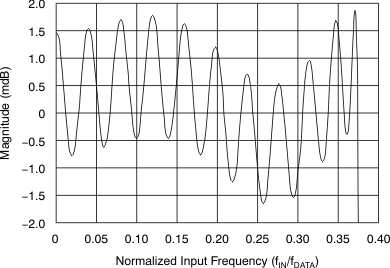
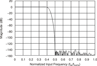
As shown in Figure 47, the frequency response of the FIR filter is minimum ripple, flat to 0.375 of the data rate (±0.003 dB pass-band ripple until 0.375 · fDATA) and is fully attenuated at the Nyquist frequency. Figure 48 shows the transition from pass band to stop band.
 Figure 47. FIR Pass-Band Magnitude Response
  Figure 48. FIR Transition Band Magnitude Response
 Although not shown in Figure 48, the pass-band response repeats at multiples of the modulator frequency (N · fMOD – f0 and N · fMOD + f0, where N = 1, 2, and so on, and f0 = pass band). These image frequencies, if present in the signal and not filtered before the analog-to-digital conversion process, fold back (or alias) into the pass band and cause errors. A low-pass signal filter reduces the amplitude of the aliasing frequencies. Often, the RC low-pass filter provided by the PGA output resistance and the external capacitor connected to CAPP and CAPN provide sufficient anti-alias attenuation.