ZHCSIU4A September 2018 – August 2019 ADS1284
PRODUCTION DATA.
- 1 特性
- 2 应用
- 3 说明
- 4 修订历史记录
- 5 Pin Configuration and Functions
- 6 Specifications
- 7 Parameter Measurement Information
-
8 Detailed Description
- 8.1 Overview
- 8.2 Functional Block Diagram
- 8.3 Feature Description
- 8.4
Device Functional Modes
- 8.4.1 Synchronization (SYNC PIN and SYNC Command)
- 8.4.2 Reset (RESET Pin and Reset Command)
- 8.4.3 Master Clock Input (CLK)
- 8.4.4 Power-Down (PWDN Pin and STANDBY Command)
- 8.4.5 Power-On Sequence
- 8.4.6 DVDD Power Supply
- 8.4.7 Serial Interface
- 8.4.8 Data Format
- 8.4.9 Reading Data
- 8.4.10 One-Shot Operation
- 8.4.11 Offset and Full-Scale Calibration Registers
- 8.4.12 Calibration Commands (OFSCAL and GANCAL)
- 8.4.13 User Calibration
- 8.5
Programming
- 8.5.1
Commands
- 8.5.1.1 SDATAC Requirements
- 8.5.1.2 WAKEUP: Wake-Up From Standby Mode
- 8.5.1.3 STANDBY: Standby Mode
- 8.5.1.4 SYNC: Synchronize the Analog-to-Digital Conversion
- 8.5.1.5 RESET: Reset the Device
- 8.5.1.6 RDATAC: Read Data Continuous
- 8.5.1.7 SDATAC: Stop Read Data Continuous
- 8.5.1.8 RDATA: Read Data by Command
- 8.5.1.9 RREG: Read Register Data
- 8.5.1.10 WREG: Write to Register
- 8.5.1.11 OFSCAL: Offset Calibration
- 8.5.1.12 GANCAL: Gain Calibration
- 8.5.1
Commands
- 8.6
Register Maps
- 8.6.1
Register Descriptions
- 8.6.1.1 ID_CFG: ID_Configuration Register (address = 00h) [reset =x0h]
- 8.6.1.2 CONFIG0: Configuration Register 0 (address = 01h) [reset = 52h]
- 8.6.1.3 CONFIG1: Configuration Register 1 (address = 02h) [reset = 08h]
- 8.6.1.4 HPF0 and HPF1 Registers
- 8.6.1.5 OFC0, OFC1, OFC2 Registers
- 8.6.1.6 FSC0, FSC1, FSC2 Registers
- 8.6.1
Register Descriptions
- 9 Application and Implementation
- 10器件和文档支持
- 11机械、封装和可订购信息
8.3.3.2.4 HPF Section
The last section of the digital filter is a first-order HPF implemented as an IIR structure. This filter stage blocks dc signals, and rolls-off low frequency components below the cutoff frequency. The transfer function for the filter is shown in Equation 11:

The high-pass corner frequency is programmed by registers HPF[1:0], in hexadecimal. Equation 13 is used to set the high-pass corner frequency. Table 13 lists example values for the high-pass filter.

where
- HPF[1:0] = High-pass filter register value (converted to hexadecimal)
- ωN = 2πfHP / fDATA (normalized frequency, radians)
- fHP = High-pass corner frequency (Hz)
- fDATA = Data rate (Hz)
Table 13. High-Pass Filter Value Examples
| fHP (Hz) | DATA RATE (SPS) | HPF[1:0] |
|---|---|---|
| 0.5 | 250 | 0337h |
| 1.0 | 500 | 0337h |
| 1.0 | 1000 | 019Ah |
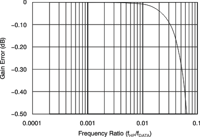
The HPF causes a small gain error, in which case the magnitude of the error depends on the ratio of fHP / fDATA. For many common values of (fHP / fDATA), the gain error is negligible. Figure 51 shows the gain error of the HPF.
 Figure 51. HPF Gain Error
 The gain error factor is calculated in Equation 14:

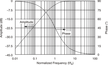
Figure 52 shows the first-order amplitude and phase response of the HPF. In the case of applying step inputs (changing gains or inputs) or synchronizing, make sure to take the settling time of the filter into account.
 Figure 52. HPF Amplitude and Phase Response