ZHCSK67B June   2017  – August 2019 ADS1287

PRODUCTION DATA.  

  1. 特性
  2. 应用
  3. 说明
    1.     Device Images
      1.      功能方框图
  4. 修订历史记录
  5. Pin Configuration and Functions
    1.     Pin Functions
  6. Specifications
    1. 6.1 Absolute Maximum Ratings
    2. 6.2 ESD Ratings
    3. 6.3 Recommended Operating Conditions
    4. 6.4 Thermal Information
    5. 6.5 Electrical Characteristics
    6. 6.6 Timing Requirements
    7. 6.7 Switching Characteristics
    8. 6.8 Typical Characteristics
  7. Parameter Measurement Information
    1. 7.1 Noise Performance
  8. Detailed Description
    1. 8.1 Overview
    2. 8.2 Functional Block Diagram
    3. 8.3 Feature Description
      1. 8.3.1 Analog Input and Multiplexer
      2. 8.3.2 Programmable Gain Amplifier (PGA)
      3. 8.3.3 Modulator
        1. 8.3.3.1 Modulator Overrange
      4. 8.3.4 Voltage Reference Inputs (REFP, REFN)
      5. 8.3.5 Digital Filter
        1. 8.3.5.1 Sinc Filter Stage
        2. 8.3.5.2 FIR Filter Stage
        3. 8.3.5.3 Group Delay and Step Response
          1. 8.3.5.3.1 Linear Phase Response
          2. 8.3.5.3.2 Minimum Phase Response
        4. 8.3.5.4 HPF Stage
      6. 8.3.6 Reset (RESET Pin and Reset Command)
      7. 8.3.7 Master Clock Input (CLK)
    4. 8.4 Device Functional Modes
      1. 8.4.1  Operational Mode
      2. 8.4.2  Chop Mode
      3. 8.4.3  Offset
      4. 8.4.4  Power-Down Mode
      5. 8.4.5  Standby Mode
      6. 8.4.6  Synchronization
        1. 8.4.6.1 Pulse-Sync Mode
        2. 8.4.6.2 Continuous-Sync Mode
      7. 8.4.7  Reading Data
        1. 8.4.7.1 Read-Data-Continuous Mode (RDATAC)
        2. 8.4.7.2 Stop-Read-Data-Continuous-Mode (SDATAC)
      8. 8.4.8  Conversion Data Format
      9. 8.4.9  Offset and Full-Scale Calibration Registers
        1. 8.4.9.1 OFC[2:0] Registers
        2. 8.4.9.2 FSC[2:0] Registers
      10. 8.4.10 Calibration Command
        1. 8.4.10.1 OFSCAL Command
        2. 8.4.10.2 GANCAL Command
      11. 8.4.11 User Calibration
    5. 8.5 Programming
      1. 8.5.1 Serial Interface
        1. 8.5.1.1 Chip Select (CS)
        2. 8.5.1.2 Serial Clock (SCLK)
        3. 8.5.1.3 Data Input (DIN)
        4. 8.5.1.4 Data Output (DOUT)
        5. 8.5.1.5 Serial Interface Timeout
        6. 8.5.1.6 Data Ready (DRDY)
      2. 8.5.2 Commands
        1. 8.5.2.1  WAKEUP: Wake Up Command
        2. 8.5.2.2  STANDBY: Standby Mode Command
        3. 8.5.2.3  SYNC: Synchronize ADC Conversions
        4. 8.5.2.4  RESET: Reset Command
        5. 8.5.2.5  RDATAC: Read Data Continuous Mode Command
        6. 8.5.2.6  SDATAC: Stop Read Data Continuous Mode Command
        7. 8.5.2.7  RDATA: Read Data Command
        8. 8.5.2.8  RREG: Read Register Data Command
        9. 8.5.2.9  WREG: Write Register Data Command
        10. 8.5.2.10 OFSCAL: Offset Calibration Command
        11. 8.5.2.11 GANCAL: Gain Calibration Command
    6. 8.6 Register Map
      1. 8.6.1 Register Descriptions
        1. 8.6.1.1 ID/CFG: ID, Configuration Register (address = 00h) [reset = x0h]
          1. Table 22. ID/CFG Register Field Descriptions
        2. 8.6.1.2 CONFIG0: Configuration Register 0 (address = 01h) [reset = 52h]
          1. Table 23. CONFIG0 Register Field Descriptions
        3. 8.6.1.3 CONFIG1: Configuration Register 1 (address = 02h) [reset = 08h]
          1. Table 24. CONFIG1 Register Field Descriptions
        4. 8.6.1.4 High-Pass Filter Corner Frequency (HPFx) Registers (address = 03h, 04h) [reset = 32h, 03h]
          1. Table 25. HPF0, HPF1 Registers Field Description
        5. 8.6.1.5 Offset Calibration (OFCx) Registers (address = 05h, 06h, 07h) [reset = 00h, 00h, 00h]
          1. Table 26. OFC0, OFC1, OFC2 Registers Field Description
        6. 8.6.1.6 Full-Scale Calibration (FSCx) Registers (address = 08h, 09h, 0Ah) [reset = 00h, 00h, 40h]
          1. Table 27. FSC0, FSC1, FSC2 Registers Field Description
  9. Application and Implementation
    1. 9.1 Application Information
    2. 9.2 Typical Applications
      1. 9.2.1 Geophone Application
      2. 9.2.2 Digital Interface
    3. 9.3 Initialization Set Up
  10. 10Power Supply Recommendations
    1. 10.1 Analog Power Supplies
    2. 10.2 Digital Power Supply
    3. 10.3 Power-Supply Sequence
  11. 11Layout
    1. 11.1 Layout Guidelines
  12. 12器件和文档支持
    1. 12.1 接收文档更新通知
    2. 12.2 社区资源
    3. 12.3 商标
    4. 12.4 静电放电警告
    5. 12.5 Glossary
  13. 13机械、封装和可订购信息

封装选项

请参考 PDF 数据表获取器件具体的封装图。

机械数据 (封装 | 引脚)
  • RHF|24
散热焊盘机械数据 (封装 | 引脚)
订购信息

Typical Characteristics

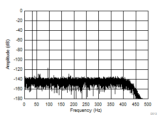
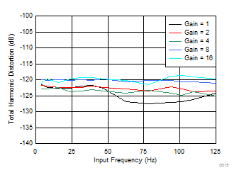
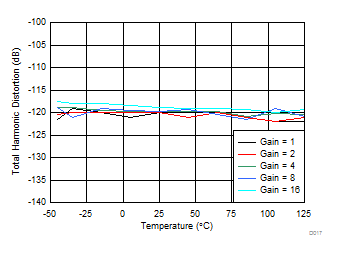
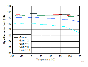
at TA = 25°C, AVDD = 2.5 V, AVSS = –2.5 V, DVDD = 3.3 V, fCLK = 1.024 MHz, V(REFP) = 0 V, V(REFN) = –2.5 V, gain = 1, high-resolution and low-power modes, chop enabled, offset disabled, and fDATA = 1000 SPS (unless otherwise noted)
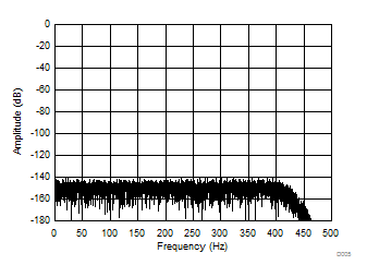
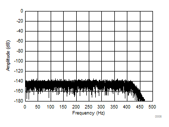
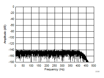
ADS1287 D005_SBAS778.gif
Shorted input, high-resolution mode,
gain = 1, 8192 points, SNR = 113.2 dB
Figure 8. Output Spectrum
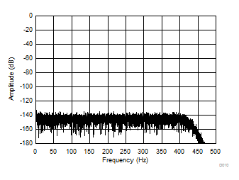
ADS1287 D009_SBAS778.gif
Shorted input, chop disabled, high-resolution mode,
gain = 8, 8192 points, SNR = 111.3 dB
Figure 10. Output Spectrum
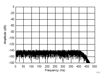
ADS1287 D008_SBAS778.gif
Shorted input, low-power mode, offset enabled,
gain = 8, 8192 points, SNR = 108.4 dB
Figure 12. Output Spectrum
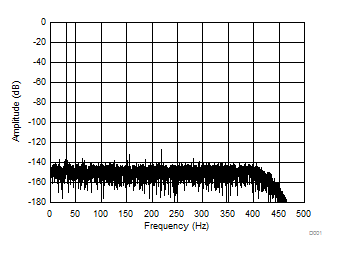
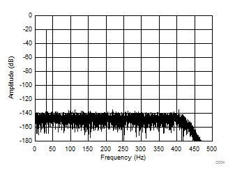
ADS1287 D001_SBAS778.gif
fIN = 31.25 Hz, –0.5 dB, high-resolution mode,
gain = 1, 8192 points
Figure 14. Output Spectrum
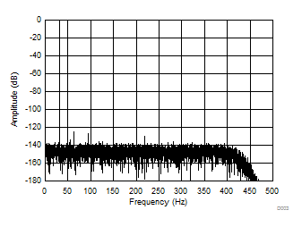
ADS1287 D003_SBAS778.gif
fIN = 31.25 Hz, –0.5 dB, high-resolution mode,
gain = 8, 8192 points
Figure 16. Output Spectrum
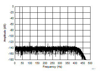
ADS1287 D011_SBAS778.gif
fIN = 31.25 Hz, –0.5 dB, low-power mode,
gain = 1, 8192 points
Figure 18. Output Spectrum
ADS1287 D013_SBAS778.gif
fIN = 31.25 Hz, –0.5 dB, low-power mode,
gain = 8, 8192 points
Figure 20. Output Spectrum
ADS1287 D015_SBAS778.gif
High-resolution mode, VIN = –0.5 dB
Figure 22. THD vs Input Frequency
ADS1287 D017_SBAS778.gif
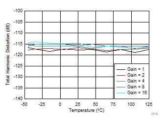
fIN = 31.25 Hz, –0.5 dB, high-resolution mode
Figure 24. THD vs Temperature
ADS1287 D019_SBAS778.gif
Shorted input, high-resolution mode
Figure 26. SNR vs Temperature
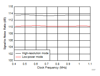
ADS1287 D027_SBAS778.gif
Shorted input
Figure 28. SNR vs Clock Frequency
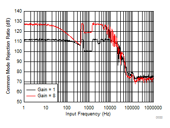
ADS1287 D022_SBAS778.gif
Low-power mode
Figure 30. CMRR vs Frequency
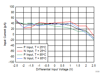
ADS1287 D028_SBAS778.gif
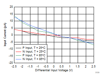
Chop enabled, gain = 1, high-resolution mode
Figure 32. Input Current vs Input Voltage
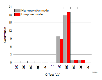
ADS1287 D034_SBAS778.gif
Chop enabled, gain = 1, 30 units
Figure 34. Offset Error Histogram
ADS1287 D035_SBAS778.gif
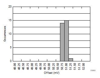
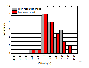
Offset enabled (50 mV), low-power mode,
gain = 1, 30 units
Figure 36. Offset Error Histogram
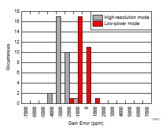
ADS1287 D031_SBAS778.gif
Gain = 1, 30 units
Figure 38. Gain Error Histogram
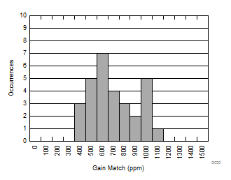
ADS1287 D030_SBAS778.gif
Gain = 2, 4, 8, 16 match to gain = 1;
30 units
Figure 40. Gain Match Error Histogram
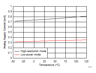
ADS1287 D024_SBAS778.gif
Figure 42. Analog Supply Current vs Temperature
ADS1287 D006_SBAS778.gif
Shorted input, high-resolution mode,
gain = 8, 8192 points, SNR = 111.8 dB
Figure 9. Output Spectrum
ADS1287 D007_SBAS778.gif
Shorted input, low-power mode, offset enabled,
gain = 1, 8192 points, SNR = 110.1 dB
Figure 11. Output Spectrum
ADS1287 D010_SBAS778.gif
Shorted input, low-power mode, chop disabled,
gain = 8, 8192 points, SNR = 108.0 dB
Figure 13. Output Spectrum
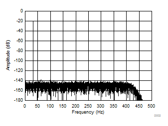
ADS1287 D002_SBAS778.gif
fIN = 31.25 Hz, –20 dB, high-resolution mode,
gain = 1, 8192 points
Figure 15. Output Spectrum
ADS1287 D004_SBAS778.gif
fIN = 31.25 Hz, –20 dB, high-resolution mode,
gain = 8, 8192 points
Figure 17. Output Spectrum
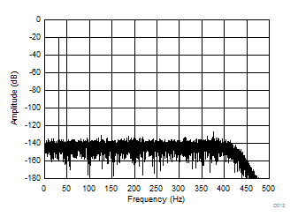
ADS1287 D012_SBAS778.gif
fIN = 31.25 Hz, –20 dB, low-power mode,
gain = 1, 8192 points
Figure 19. Output Spectrum
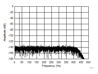
ADS1287 D014_SBAS778.gif
fIN = 31.25 Hz, –20 dB, low-power mode,
gain = 8, 8192 points
Figure 21. Output Spectrum
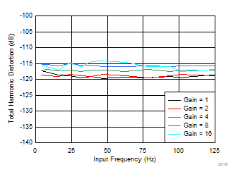
ADS1287 D016_SBAS778.gif
Low-power mode, VIN = –0.5 dB
Figure 23. THD vs Input Frequency
ADS1287 D018_SBAS778.gif
fIN = 31.25 Hz, –0.5 dB, low-power mode
Figure 25. THD vs Temperature
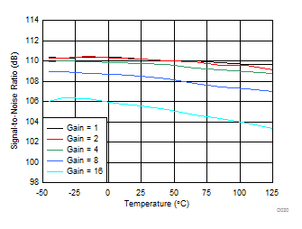
ADS1287 D020_SBAS778.gif
Shorted input, low-power mode
Figure 27. SNR vs Temperature
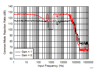
ADS1287 D021_SBAS778.gif
High-resolution mode
Figure 29. CMRR vs Frequency
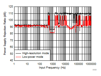
ADS1287 D023_SBAS778.gif
Figure 31. Analog Supply PSRR vs Frequency
ADS1287 D029_SBAS778.gif
Chop disabled, gain = 1, high-resolution mode
Figure 33. Input Current vs Input Voltage
ADS1287 D033_SBAS778.gif
Chop disabled, gain = 1, 30 units
Figure 35. Offset Error Histogram
ADS1287 D036_SBAS778.gif
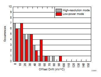
Chop enabled, gain = 1, 30 units
Figure 37. Offset Temperature Drift Histogram
ADS1287 D032_SBAS778.gif
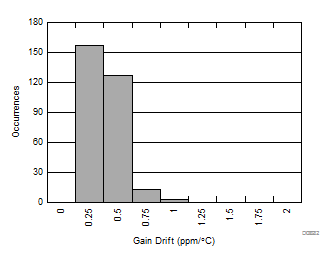
Gain = 1, 2, 4, 8 and 16 combined; 30 units;
combined high-resolution and low-power modes
Figure 39. Gain Drift Histogram
ADS1287 D025_SBAS778.gif
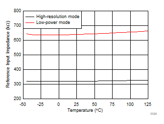
Figure 41. Reference Input Impedance vs Temperature
ADS1287 D026_SBAS778.gif
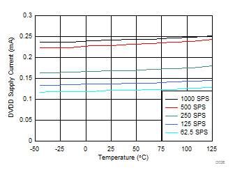
High-resolution mode
Figure 43. Digital Supply Current vs Temperature