ZHCSK67B June 2017 – August 2019 ADS1287
PRODUCTION DATA.
- 1 特性
- 2 应用
- 3 说明
- 4 修订历史记录
- 5 Pin Configuration and Functions
- 6 Specifications
- 7 Parameter Measurement Information
-
8 Detailed Description
- 8.1 Overview
- 8.2 Functional Block Diagram
- 8.3 Feature Description
- 8.4 Device Functional Modes
- 8.5
Programming
- 8.5.1 Serial Interface
- 8.5.2
Commands
- 8.5.2.1 WAKEUP: Wake Up Command
- 8.5.2.2 STANDBY: Standby Mode Command
- 8.5.2.3 SYNC: Synchronize ADC Conversions
- 8.5.2.4 RESET: Reset Command
- 8.5.2.5 RDATAC: Read Data Continuous Mode Command
- 8.5.2.6 SDATAC: Stop Read Data Continuous Mode Command
- 8.5.2.7 RDATA: Read Data Command
- 8.5.2.8 RREG: Read Register Data Command
- 8.5.2.9 WREG: Write Register Data Command
- 8.5.2.10 OFSCAL: Offset Calibration Command
- 8.5.2.11 GANCAL: Gain Calibration Command
- 8.6
Register Map
- 8.6.1
Register Descriptions
- 8.6.1.1 ID/CFG: ID, Configuration Register (address = 00h) [reset = x0h]
- 8.6.1.2 CONFIG0: Configuration Register 0 (address = 01h) [reset = 52h]
- 8.6.1.3 CONFIG1: Configuration Register 1 (address = 02h) [reset = 08h]
- 8.6.1.4 High-Pass Filter Corner Frequency (HPFx) Registers (address = 03h, 04h) [reset = 32h, 03h]
- 8.6.1.5 Offset Calibration (OFCx) Registers (address = 05h, 06h, 07h) [reset = 00h, 00h, 00h]
- 8.6.1.6 Full-Scale Calibration (FSCx) Registers (address = 08h, 09h, 0Ah) [reset = 00h, 00h, 40h]
- 8.6.1
Register Descriptions
- 9 Application and Implementation
- 10Power Supply Recommendations
- 11Layout
- 12器件和文档支持
- 13机械、封装和可订购信息
8.3.1 Analog Input and Multiplexer
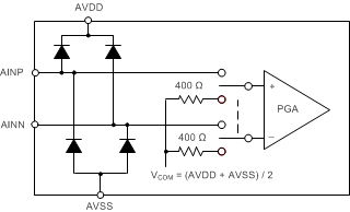
Figure 44 shows a diagram of the analog input circuit and multiplexer.
 Figure 44. Analog Input and Multiplexer
 Electrostatic discharge (ESD) diodes are incorporated to protect the ADC inputs from ESD exposure that can occur during device manufacturing and printed circuit board (PCB) assembly process when assembled in an ESD-controlled environment. For system-level ESD protection, external ESD protection devices are recommended to protect device inputs or outputs that may be exposed to ESD events.
If either input is taken below AVSS – 0.3 V, or above AVDD + 0.3 V, the internal protection diodes can conduct. If these conditions are possible, use external clamp diodes, series resistors, or both to limit the maximum input current to the specified value.
The input multiplexer selects between the external input or the internal (shorted) input. The internal short is via two 400-Ω resistors to analog mid-supply voltage (VCOM). The thermal noise of the resistors is equivalent to the noise produced by common geophones. Use the internal short connection to verify the ADC offset voltage and noise performance, and to provide an input to calibrate the ADC offset voltage. Table 5 summarizes the register selections of the multiplexer configurations related to Figure 44.
Table 5. Input Multiplexer Modes
| MUX[1:0] REGISTER BITS | DESCRIPTION |
|---|---|
| 00 | External input (default) |
| 01 | Reserved |
| 10 | Internal short; PGA input connected to internal VCOM voltage via 400-Ω resistors |
| 11 | Reserved |