ZHCSK67B June 2017 – August 2019 ADS1287
PRODUCTION DATA.
- 1 特性
- 2 应用
- 3 说明
- 4 修订历史记录
- 5 Pin Configuration and Functions
- 6 Specifications
- 7 Parameter Measurement Information
-
8 Detailed Description
- 8.1 Overview
- 8.2 Functional Block Diagram
- 8.3 Feature Description
- 8.4 Device Functional Modes
- 8.5
Programming
- 8.5.1 Serial Interface
- 8.5.2
Commands
- 8.5.2.1 WAKEUP: Wake Up Command
- 8.5.2.2 STANDBY: Standby Mode Command
- 8.5.2.3 SYNC: Synchronize ADC Conversions
- 8.5.2.4 RESET: Reset Command
- 8.5.2.5 RDATAC: Read Data Continuous Mode Command
- 8.5.2.6 SDATAC: Stop Read Data Continuous Mode Command
- 8.5.2.7 RDATA: Read Data Command
- 8.5.2.8 RREG: Read Register Data Command
- 8.5.2.9 WREG: Write Register Data Command
- 8.5.2.10 OFSCAL: Offset Calibration Command
- 8.5.2.11 GANCAL: Gain Calibration Command
- 8.6
Register Map
- 8.6.1
Register Descriptions
- 8.6.1.1 ID/CFG: ID, Configuration Register (address = 00h) [reset = x0h]
- 8.6.1.2 CONFIG0: Configuration Register 0 (address = 01h) [reset = 52h]
- 8.6.1.3 CONFIG1: Configuration Register 1 (address = 02h) [reset = 08h]
- 8.6.1.4 High-Pass Filter Corner Frequency (HPFx) Registers (address = 03h, 04h) [reset = 32h, 03h]
- 8.6.1.5 Offset Calibration (OFCx) Registers (address = 05h, 06h, 07h) [reset = 00h, 00h, 00h]
- 8.6.1.6 Full-Scale Calibration (FSCx) Registers (address = 08h, 09h, 0Ah) [reset = 00h, 00h, 40h]
- 8.6.1
Register Descriptions
- 9 Application and Implementation
- 10Power Supply Recommendations
- 11Layout
- 12器件和文档支持
- 13机械、封装和可订购信息
8.3.2 Programmable Gain Amplifier (PGA)
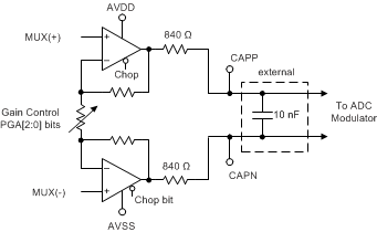
The ADC incorporates a low-noise PGA in order to extend the ADC dynamic range. The PGA is a CMOS, differential-input and differential-output amplifier. The gain factor is programmable from 1 V/V to 16 V/V and is controlled by the GAIN[2:0] register bits. The PGA differentially drives the modulator via two 840-Ω internal resistors. Connect a 10-nF, C0G-dielectric capacitor between the CAPP and CAPN pins. The capacitor filters the modulator sampling glitches and also functions as a first-order antialias filter. Equation 2 gives the corner frequency of the antialias filter:
As shown in Figure 45, the PGA is composed of two amplifiers. The amplifiers are chopper-stabilized in order to reduce the PGA 1/f noise, offset, and offset drift. The PGA chop mode can be disabled when used with certain types of high-impedance sensors, such as hydrophones; see the Chop Mode section for more details.
 Figure 45. PGA Block Diagram
 The PGA gain factors are programmable from 1 to 16 V/V. Table 6 shows the register bit setting for the PGA gain and corresponding input voltage range.
Table 6. PGA Gain Factors
| GAIN[2:0] REGISTER BITS | GAIN (V/V) | DIFFERENTIAL INPUT RANGE |
|---|---|---|
| 000 | 1 | ±2.5 V |
| 001 | 2 | ±1.25 V |
| 010 | 4 | ±0.625 V |
| 011 | 8 | ±0.3125 V |
| 100 | 16 | ±0.15625 V |
| 101 - 111 | Reserved | — |
To maintain linear operation, observe the specified PGA input and PGA output voltage range requirements. The absolute voltage is defined as the sum of the signal component plus offset voltage (common-mode voltage). Equation 3 shows the specified absolute input voltage range:
Equation 4 shows the specified absolute PGA output voltage range:
Equation 5 shows that the PGA output voltage is equal to the absolute PGA input voltage plus and minus the differential input voltage times half the PGA gain factor minus 1: