ZHCSK67B June   2017  – August 2019 ADS1287

PRODUCTION DATA.  

  1. 特性
  2. 应用
  3. 说明
    1.     Device Images
      1.      功能方框图
  4. 修订历史记录
  5. Pin Configuration and Functions
    1.     Pin Functions
  6. Specifications
    1. 6.1 Absolute Maximum Ratings
    2. 6.2 ESD Ratings
    3. 6.3 Recommended Operating Conditions
    4. 6.4 Thermal Information
    5. 6.5 Electrical Characteristics
    6. 6.6 Timing Requirements
    7. 6.7 Switching Characteristics
    8. 6.8 Typical Characteristics
  7. Parameter Measurement Information
    1. 7.1 Noise Performance
  8. Detailed Description
    1. 8.1 Overview
    2. 8.2 Functional Block Diagram
    3. 8.3 Feature Description
      1. 8.3.1 Analog Input and Multiplexer
      2. 8.3.2 Programmable Gain Amplifier (PGA)
      3. 8.3.3 Modulator
        1. 8.3.3.1 Modulator Overrange
      4. 8.3.4 Voltage Reference Inputs (REFP, REFN)
      5. 8.3.5 Digital Filter
        1. 8.3.5.1 Sinc Filter Stage
        2. 8.3.5.2 FIR Filter Stage
        3. 8.3.5.3 Group Delay and Step Response
          1. 8.3.5.3.1 Linear Phase Response
          2. 8.3.5.3.2 Minimum Phase Response
        4. 8.3.5.4 HPF Stage
      6. 8.3.6 Reset (RESET Pin and Reset Command)
      7. 8.3.7 Master Clock Input (CLK)
    4. 8.4 Device Functional Modes
      1. 8.4.1  Operational Mode
      2. 8.4.2  Chop Mode
      3. 8.4.3  Offset
      4. 8.4.4  Power-Down Mode
      5. 8.4.5  Standby Mode
      6. 8.4.6  Synchronization
        1. 8.4.6.1 Pulse-Sync Mode
        2. 8.4.6.2 Continuous-Sync Mode
      7. 8.4.7  Reading Data
        1. 8.4.7.1 Read-Data-Continuous Mode (RDATAC)
        2. 8.4.7.2 Stop-Read-Data-Continuous-Mode (SDATAC)
      8. 8.4.8  Conversion Data Format
      9. 8.4.9  Offset and Full-Scale Calibration Registers
        1. 8.4.9.1 OFC[2:0] Registers
        2. 8.4.9.2 FSC[2:0] Registers
      10. 8.4.10 Calibration Command
        1. 8.4.10.1 OFSCAL Command
        2. 8.4.10.2 GANCAL Command
      11. 8.4.11 User Calibration
    5. 8.5 Programming
      1. 8.5.1 Serial Interface
        1. 8.5.1.1 Chip Select (CS)
        2. 8.5.1.2 Serial Clock (SCLK)
        3. 8.5.1.3 Data Input (DIN)
        4. 8.5.1.4 Data Output (DOUT)
        5. 8.5.1.5 Serial Interface Timeout
        6. 8.5.1.6 Data Ready (DRDY)
      2. 8.5.2 Commands
        1. 8.5.2.1  WAKEUP: Wake Up Command
        2. 8.5.2.2  STANDBY: Standby Mode Command
        3. 8.5.2.3  SYNC: Synchronize ADC Conversions
        4. 8.5.2.4  RESET: Reset Command
        5. 8.5.2.5  RDATAC: Read Data Continuous Mode Command
        6. 8.5.2.6  SDATAC: Stop Read Data Continuous Mode Command
        7. 8.5.2.7  RDATA: Read Data Command
        8. 8.5.2.8  RREG: Read Register Data Command
        9. 8.5.2.9  WREG: Write Register Data Command
        10. 8.5.2.10 OFSCAL: Offset Calibration Command
        11. 8.5.2.11 GANCAL: Gain Calibration Command
    6. 8.6 Register Map
      1. 8.6.1 Register Descriptions
        1. 8.6.1.1 ID/CFG: ID, Configuration Register (address = 00h) [reset = x0h]
          1. Table 22. ID/CFG Register Field Descriptions
        2. 8.6.1.2 CONFIG0: Configuration Register 0 (address = 01h) [reset = 52h]
          1. Table 23. CONFIG0 Register Field Descriptions
        3. 8.6.1.3 CONFIG1: Configuration Register 1 (address = 02h) [reset = 08h]
          1. Table 24. CONFIG1 Register Field Descriptions
        4. 8.6.1.4 High-Pass Filter Corner Frequency (HPFx) Registers (address = 03h, 04h) [reset = 32h, 03h]
          1. Table 25. HPF0, HPF1 Registers Field Description
        5. 8.6.1.5 Offset Calibration (OFCx) Registers (address = 05h, 06h, 07h) [reset = 00h, 00h, 00h]
          1. Table 26. OFC0, OFC1, OFC2 Registers Field Description
        6. 8.6.1.6 Full-Scale Calibration (FSCx) Registers (address = 08h, 09h, 0Ah) [reset = 00h, 00h, 40h]
          1. Table 27. FSC0, FSC1, FSC2 Registers Field Description
  9. Application and Implementation
    1. 9.1 Application Information
    2. 9.2 Typical Applications
      1. 9.2.1 Geophone Application
      2. 9.2.2 Digital Interface
    3. 9.3 Initialization Set Up
  10. 10Power Supply Recommendations
    1. 10.1 Analog Power Supplies
    2. 10.2 Digital Power Supply
    3. 10.3 Power-Supply Sequence
  11. 11Layout
    1. 11.1 Layout Guidelines
  12. 12器件和文档支持
    1. 12.1 接收文档更新通知
    2. 12.2 社区资源
    3. 12.3 商标
    4. 12.4 静电放电警告
    5. 12.5 Glossary
  13. 13机械、封装和可订购信息

封装选项

请参考 PDF 数据表获取器件具体的封装图。

机械数据 (封装 | 引脚)
  • RHF|24
散热焊盘机械数据 (封装 | 引脚)
订购信息

Sinc Filter Stage

The sinc filter (sinx/x) is a variable-decimation, fifth-order, low-pass filter. Data are supplied to this filter from the modulator at the rate of fMOD = fCLK / 4 (high-resolution mode), fCLK / 8 (low-power mode). The sinc filter attenuates the high-frequency noise of the modulator. The sinc filter provides down-sampled, partially-filtered data to the FIR filter. The decimation ratio of the sinc filter is variable and determines the overall data rate. Table 8 shows that the decimation ratio of the sinc filter is programmed by the DR[2:0] register bits.

Table 8. Sinc Filter Data Rates

DR[2:0] REGISTER BITS SINC DECIMATION RATIO (N) SINC DATA RATE (SPS)
HIGH-RESOLUTION MODE LOW-POWER MODE
000 128 64 2,000
001 64 32 4,000
010 32 16 8,000
011 16 8 16,000
100 8 4 32,000
101 - 111 Reserved Reserved Reserved

Equation 8 shows the scaled Z-domain transfer function of the sinc filter.

Equation 8. ADS1287 q_hz_bas418.gif

where

  • N = decimation ratio

Equation 9 shows the frequency domain transfer function of the sinc filter.
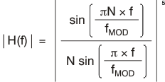
Equation 9. ADS1287 q_hf_bas418.gif

where

  • N = Decimation ratio (see Table 8)
  • f = Input signal frequency
  • fMOD = Modulator sampling frequency = fCLK / 4 (high resolution mode), fCLK / 8 (low-power mode)

The frequency response of the sinc filter contains notches (or zeros) that occur at the output data rate frequency and multiples thereof. At these frequencies, the filter has zero gain. Figure 49 shows the wide-band frequency response of the sinc filter and Figure 50 shows the –3-dB response.
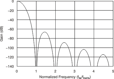
ADS1287 ai_sinc_gain-freq_bas418.gifFigure 49. Sinc Filter Frequency Response
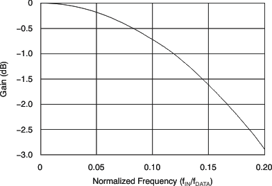
ADS1287 ai_sinc_rolloff_bas418.gifFigure 50. Sinc Filter –3-dB Response