ZHCSK67B June   2017  – August 2019 ADS1287

PRODUCTION DATA.  

  1. 特性
  2. 应用
  3. 说明
    1.     Device Images
      1.      功能方框图
  4. 修订历史记录
  5. Pin Configuration and Functions
    1.     Pin Functions
  6. Specifications
    1. 6.1 Absolute Maximum Ratings
    2. 6.2 ESD Ratings
    3. 6.3 Recommended Operating Conditions
    4. 6.4 Thermal Information
    5. 6.5 Electrical Characteristics
    6. 6.6 Timing Requirements
    7. 6.7 Switching Characteristics
    8. 6.8 Typical Characteristics
  7. Parameter Measurement Information
    1. 7.1 Noise Performance
  8. Detailed Description
    1. 8.1 Overview
    2. 8.2 Functional Block Diagram
    3. 8.3 Feature Description
      1. 8.3.1 Analog Input and Multiplexer
      2. 8.3.2 Programmable Gain Amplifier (PGA)
      3. 8.3.3 Modulator
        1. 8.3.3.1 Modulator Overrange
      4. 8.3.4 Voltage Reference Inputs (REFP, REFN)
      5. 8.3.5 Digital Filter
        1. 8.3.5.1 Sinc Filter Stage
        2. 8.3.5.2 FIR Filter Stage
        3. 8.3.5.3 Group Delay and Step Response
          1. 8.3.5.3.1 Linear Phase Response
          2. 8.3.5.3.2 Minimum Phase Response
        4. 8.3.5.4 HPF Stage
      6. 8.3.6 Reset (RESET Pin and Reset Command)
      7. 8.3.7 Master Clock Input (CLK)
    4. 8.4 Device Functional Modes
      1. 8.4.1  Operational Mode
      2. 8.4.2  Chop Mode
      3. 8.4.3  Offset
      4. 8.4.4  Power-Down Mode
      5. 8.4.5  Standby Mode
      6. 8.4.6  Synchronization
        1. 8.4.6.1 Pulse-Sync Mode
        2. 8.4.6.2 Continuous-Sync Mode
      7. 8.4.7  Reading Data
        1. 8.4.7.1 Read-Data-Continuous Mode (RDATAC)
        2. 8.4.7.2 Stop-Read-Data-Continuous-Mode (SDATAC)
      8. 8.4.8  Conversion Data Format
      9. 8.4.9  Offset and Full-Scale Calibration Registers
        1. 8.4.9.1 OFC[2:0] Registers
        2. 8.4.9.2 FSC[2:0] Registers
      10. 8.4.10 Calibration Command
        1. 8.4.10.1 OFSCAL Command
        2. 8.4.10.2 GANCAL Command
      11. 8.4.11 User Calibration
    5. 8.5 Programming
      1. 8.5.1 Serial Interface
        1. 8.5.1.1 Chip Select (CS)
        2. 8.5.1.2 Serial Clock (SCLK)
        3. 8.5.1.3 Data Input (DIN)
        4. 8.5.1.4 Data Output (DOUT)
        5. 8.5.1.5 Serial Interface Timeout
        6. 8.5.1.6 Data Ready (DRDY)
      2. 8.5.2 Commands
        1. 8.5.2.1  WAKEUP: Wake Up Command
        2. 8.5.2.2  STANDBY: Standby Mode Command
        3. 8.5.2.3  SYNC: Synchronize ADC Conversions
        4. 8.5.2.4  RESET: Reset Command
        5. 8.5.2.5  RDATAC: Read Data Continuous Mode Command
        6. 8.5.2.6  SDATAC: Stop Read Data Continuous Mode Command
        7. 8.5.2.7  RDATA: Read Data Command
        8. 8.5.2.8  RREG: Read Register Data Command
        9. 8.5.2.9  WREG: Write Register Data Command
        10. 8.5.2.10 OFSCAL: Offset Calibration Command
        11. 8.5.2.11 GANCAL: Gain Calibration Command
    6. 8.6 Register Map
      1. 8.6.1 Register Descriptions
        1. 8.6.1.1 ID/CFG: ID, Configuration Register (address = 00h) [reset = x0h]
          1. Table 22. ID/CFG Register Field Descriptions
        2. 8.6.1.2 CONFIG0: Configuration Register 0 (address = 01h) [reset = 52h]
          1. Table 23. CONFIG0 Register Field Descriptions
        3. 8.6.1.3 CONFIG1: Configuration Register 1 (address = 02h) [reset = 08h]
          1. Table 24. CONFIG1 Register Field Descriptions
        4. 8.6.1.4 High-Pass Filter Corner Frequency (HPFx) Registers (address = 03h, 04h) [reset = 32h, 03h]
          1. Table 25. HPF0, HPF1 Registers Field Description
        5. 8.6.1.5 Offset Calibration (OFCx) Registers (address = 05h, 06h, 07h) [reset = 00h, 00h, 00h]
          1. Table 26. OFC0, OFC1, OFC2 Registers Field Description
        6. 8.6.1.6 Full-Scale Calibration (FSCx) Registers (address = 08h, 09h, 0Ah) [reset = 00h, 00h, 40h]
          1. Table 27. FSC0, FSC1, FSC2 Registers Field Description
  9. Application and Implementation
    1. 9.1 Application Information
    2. 9.2 Typical Applications
      1. 9.2.1 Geophone Application
      2. 9.2.2 Digital Interface
    3. 9.3 Initialization Set Up
  10. 10Power Supply Recommendations
    1. 10.1 Analog Power Supplies
    2. 10.2 Digital Power Supply
    3. 10.3 Power-Supply Sequence
  11. 11Layout
    1. 11.1 Layout Guidelines
  12. 12器件和文档支持
    1. 12.1 接收文档更新通知
    2. 12.2 社区资源
    3. 12.3 商标
    4. 12.4 静电放电警告
    5. 12.5 Glossary
  13. 13机械、封装和可订购信息

封装选项

请参考 PDF 数据表获取器件具体的封装图。

机械数据 (封装 | 引脚)
  • RHF|24
散热焊盘机械数据 (封装 | 引脚)
订购信息

HPF Stage

The last stage of the digital filter is a high-pass filter (HPF) implemented as a first-order, IIR structure. This filter stage blocks DC signals and rolls off low-frequency components below the cutoff frequency. Equation 10 shows the transfer function for the filter:

Equation 10. ADS1287 q_hpf2_bas418.gif

where

Equation 11. ADS1287 q_b_bas418.gif

The high-pass filter corner frequency is programmed by the HPF[1:0] register bits, in hexadecimal. Equation 12 is used to set the high-pass filter corner frequency. Table 12 lists example values for the high-pass filter.

Equation 12. ADS1287 q_hpf1-0_bas418.gif

where

  • HPF = High-pass filter register value (converted to hexadecimal)
  • ωN = 2πfHP / fDATA (normalized frequency, radians)
  • fHP = High-pass filter corner frequency (Hz)
  • fDATA = Data rate (Hz)

Table 12. High-Pass Filter Value Examples

HPF1, HPF0 fHP (Hz) DATA RATE (SPS)
0337h 0.5 250
0337h 1.0 500
019Ah 1.0 1000

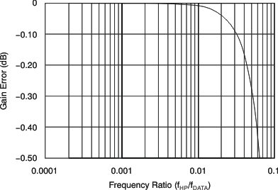
Equation 13 shows the HPF frequency domain transfer function. The HPF results in a small gain error that depends on the ratio of fHP / fDATA. For many common values of (fHP / fDATA), the gain error is negligible. Figure 56 shows the gain error of the HPF.
ADS1287 ai_hpf_g_err_bas418.gifFigure 56. HPF Gain Error
Equation 13. ADS1287 q_hpf_gerr_bas418.gif

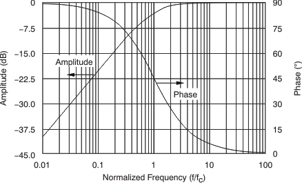
Figure 57 shows the first-order amplitude and phase response of the HPF. In the case of applied step input or after synchronizing, make sure to take the settling time of the filter into account.
ADS1287 ai_hpf_amp-freq_bas418.gifFigure 57. HPF Amplitude and Phase Response