ZHCSK67B June 2017 – August 2019 ADS1287
PRODUCTION DATA.
- 1 特性
- 2 应用
- 3 说明
- 4 修订历史记录
- 5 Pin Configuration and Functions
- 6 Specifications
- 7 Parameter Measurement Information
-
8 Detailed Description
- 8.1 Overview
- 8.2 Functional Block Diagram
- 8.3 Feature Description
- 8.4 Device Functional Modes
- 8.5
Programming
- 8.5.1 Serial Interface
- 8.5.2
Commands
- 8.5.2.1 WAKEUP: Wake Up Command
- 8.5.2.2 STANDBY: Standby Mode Command
- 8.5.2.3 SYNC: Synchronize ADC Conversions
- 8.5.2.4 RESET: Reset Command
- 8.5.2.5 RDATAC: Read Data Continuous Mode Command
- 8.5.2.6 SDATAC: Stop Read Data Continuous Mode Command
- 8.5.2.7 RDATA: Read Data Command
- 8.5.2.8 RREG: Read Register Data Command
- 8.5.2.9 WREG: Write Register Data Command
- 8.5.2.10 OFSCAL: Offset Calibration Command
- 8.5.2.11 GANCAL: Gain Calibration Command
- 8.6
Register Map
- 8.6.1
Register Descriptions
- 8.6.1.1 ID/CFG: ID, Configuration Register (address = 00h) [reset = x0h]
- 8.6.1.2 CONFIG0: Configuration Register 0 (address = 01h) [reset = 52h]
- 8.6.1.3 CONFIG1: Configuration Register 1 (address = 02h) [reset = 08h]
- 8.6.1.4 High-Pass Filter Corner Frequency (HPFx) Registers (address = 03h, 04h) [reset = 32h, 03h]
- 8.6.1.5 Offset Calibration (OFCx) Registers (address = 05h, 06h, 07h) [reset = 00h, 00h, 00h]
- 8.6.1.6 Full-Scale Calibration (FSCx) Registers (address = 08h, 09h, 0Ah) [reset = 00h, 00h, 40h]
- 8.6.1
Register Descriptions
- 9 Application and Implementation
- 10Power Supply Recommendations
- 11Layout
- 12器件和文档支持
- 13机械、封装和可订购信息
8.4.6.2 Continuous-Sync Mode
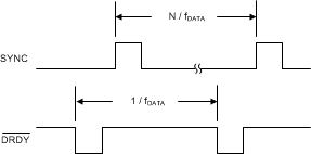
In continuous-sync mode, the ADC synchronizes on the first rising edge of the SYNC pin after configuring the ADC to the continuous-sync mode. On the subsequent rising edges of SYNC, the ADC re-synchronizes only if the SYNC input period is not equal to an integer multiple of the data rate period by at least ±1 / fCLK (that is, the SYNC period ≠ N /fDATA ± 1 /fCLK, where N = 1, 2, 3, and so forth). The period of SYNC can be indefinite. If the periods are not divisible by an integer, the ADC re-synchronizes. In this mode, a periodic synchronizing clock can be applied to the ADC, resulting in autonomous synchronization.
When synchronization occurs, DRDY continues to pulse but the ADC forces the data to zero until the data are settled (approximately 63 DRDY periods later). At the 63rd conversion, valid data are output. See Figure 4 for an illustration of DRDY behavior. The phase relationship between SYNC and DRDY also depends on the data rate because of the slight dependence of filter group delay to data rate. Figure 58 shows an example of the phase relationship between SYNC and DRDY. The SYNC pin only can be used to control continuous-sync mode.
 Figure 58. Continuous-Sync Mode
 The ADC synchronizes at the occurrence of a register write operation resulting in loss of the previous synchronization. To re-establish the previous synchronization (in continuous-sync mode), send the STANDBY, WAKEUP command sequence. The re-synchronization sequence is valid provided the time between the STANDBY and WAKEUP commands is not equal to the data rate period by at least ± 1 / fCLK period.