ZHCSK67B June 2017 – August 2019 ADS1287
PRODUCTION DATA.
- 1 特性
- 2 应用
- 3 说明
- 4 修订历史记录
- 5 Pin Configuration and Functions
- 6 Specifications
- 7 Parameter Measurement Information
-
8 Detailed Description
- 8.1 Overview
- 8.2 Functional Block Diagram
- 8.3 Feature Description
- 8.4 Device Functional Modes
- 8.5
Programming
- 8.5.1 Serial Interface
- 8.5.2
Commands
- 8.5.2.1 WAKEUP: Wake Up Command
- 8.5.2.2 STANDBY: Standby Mode Command
- 8.5.2.3 SYNC: Synchronize ADC Conversions
- 8.5.2.4 RESET: Reset Command
- 8.5.2.5 RDATAC: Read Data Continuous Mode Command
- 8.5.2.6 SDATAC: Stop Read Data Continuous Mode Command
- 8.5.2.7 RDATA: Read Data Command
- 8.5.2.8 RREG: Read Register Data Command
- 8.5.2.9 WREG: Write Register Data Command
- 8.5.2.10 OFSCAL: Offset Calibration Command
- 8.5.2.11 GANCAL: Gain Calibration Command
- 8.6
Register Map
- 8.6.1
Register Descriptions
- 8.6.1.1 ID/CFG: ID, Configuration Register (address = 00h) [reset = x0h]
- 8.6.1.2 CONFIG0: Configuration Register 0 (address = 01h) [reset = 52h]
- 8.6.1.3 CONFIG1: Configuration Register 1 (address = 02h) [reset = 08h]
- 8.6.1.4 High-Pass Filter Corner Frequency (HPFx) Registers (address = 03h, 04h) [reset = 32h, 03h]
- 8.6.1.5 Offset Calibration (OFCx) Registers (address = 05h, 06h, 07h) [reset = 00h, 00h, 00h]
- 8.6.1.6 Full-Scale Calibration (FSCx) Registers (address = 08h, 09h, 0Ah) [reset = 00h, 00h, 40h]
- 8.6.1
Register Descriptions
- 9 Application and Implementation
- 10Power Supply Recommendations
- 11Layout
- 12器件和文档支持
- 13机械、封装和可订购信息
9.2.1 Geophone Application
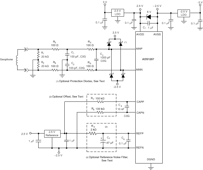
Figure 79 illustrates a typical geophone application circuit. The application shows the ADC operating on a bipolar ±2.5-V analog supply voltage. The power-supply voltages are provided by low-dropout (LDO) regulators to provide well-regulated, low-noise supply voltages to the ADC. The ADC also operates using with a unipolar 5-V analog supply voltage. The 6-V zener diode between AVDD and AVSS clamps the ADC supply voltage if the inputs are driven when the ADC supply voltage is off.
Resistors R1 and R2 bias the floating geophone to mid-supply. The resistors also provide a return path for the ADC input current. To prevent pickup of PCB ground-related noise, connect the resistors together first, then connect to ground. For unipolar-supply operation, make this connection to a low-impedance 2.5-V voltage.
The geophone signal is filtered both differentially, by components C3 and R3 through R6, and common-mode filtered by components C1, C2 and R3, R4. The differential filter removes normal-mode noise. The common-mode filters remove noise that is common to both inputs. The differential filter high-cut frequency is 10 times lower to minimize the effects of component mismatch of the common-mode filter that otherwise can lead to degraded differential-filter performance. Adjust the filter components according to the application requirements. The protection diodes protect the ADC inputs from system-level ESD transients and signal overrange events.
A low-noise, low-power, 2.5-V voltage reference drives the ADC reference input. The voltage reference ground terminal is connected to –2.5 V. R9 and C5 form an optional 2-Hz noise filter to reduce voltage reference noise. Capacitor C6 filters the reference sampling glitches. Place the capacitor directly at the ADC pins. Multiple ADCs can share a single reference but place a 0.1-µF capacitor at each ADC reference input.
Capacitor C4 (10 nF), located at the CAPP and CAPN pins, filters modulator sampling glitches. The capacitor also provides a antialiasing filter with a high cutoff corner frequency of approximately 9.5 kHz. Resistors R7 and R8 provide an offset voltage to the modulator for idle tone reduction when operating in high-resolution mode. Use the internal offset in low-power mode operation. The resistors are not needed in this case.
 Figure 79. Geophone Analog Interface