ZHCSK67B June 2017 – August 2019 ADS1287
PRODUCTION DATA.
- 1 特性
- 2 应用
- 3 说明
- 4 修订历史记录
- 5 Pin Configuration and Functions
- 6 Specifications
- 7 Parameter Measurement Information
-
8 Detailed Description
- 8.1 Overview
- 8.2 Functional Block Diagram
- 8.3 Feature Description
- 8.4 Device Functional Modes
- 8.5
Programming
- 8.5.1 Serial Interface
- 8.5.2
Commands
- 8.5.2.1 WAKEUP: Wake Up Command
- 8.5.2.2 STANDBY: Standby Mode Command
- 8.5.2.3 SYNC: Synchronize ADC Conversions
- 8.5.2.4 RESET: Reset Command
- 8.5.2.5 RDATAC: Read Data Continuous Mode Command
- 8.5.2.6 SDATAC: Stop Read Data Continuous Mode Command
- 8.5.2.7 RDATA: Read Data Command
- 8.5.2.8 RREG: Read Register Data Command
- 8.5.2.9 WREG: Write Register Data Command
- 8.5.2.10 OFSCAL: Offset Calibration Command
- 8.5.2.11 GANCAL: Gain Calibration Command
- 8.6
Register Map
- 8.6.1
Register Descriptions
- 8.6.1.1 ID/CFG: ID, Configuration Register (address = 00h) [reset = x0h]
- 8.6.1.2 CONFIG0: Configuration Register 0 (address = 01h) [reset = 52h]
- 8.6.1.3 CONFIG1: Configuration Register 1 (address = 02h) [reset = 08h]
- 8.6.1.4 High-Pass Filter Corner Frequency (HPFx) Registers (address = 03h, 04h) [reset = 32h, 03h]
- 8.6.1.5 Offset Calibration (OFCx) Registers (address = 05h, 06h, 07h) [reset = 00h, 00h, 00h]
- 8.6.1.6 Full-Scale Calibration (FSCx) Registers (address = 08h, 09h, 0Ah) [reset = 00h, 00h, 40h]
- 8.6.1
Register Descriptions
- 9 Application and Implementation
- 10Power Supply Recommendations
- 11Layout
- 12器件和文档支持
- 13机械、封装和可订购信息
9.2.2 Digital Interface
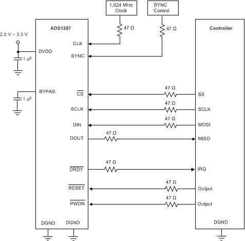
Figure 80 shows the digital connections to a controller, such as a field programmable gate array (FPGA) or microcontroller. Place the digital bypass capacitors on DVDD and the LDO output (BYPAS) close to the device pins and directly to the ground plane. Connections to the RESET andPWDN pins are optional. If not used, tie the inputs to DVDD. Avoid ringing on the digital inputs of the ADC. For long PCB traces, use 47-Ω series termination resistors to help reduce ringing by controlling the trace impedance. Place the resistors at the source (output driver).
 Figure 80. Digital Connections