ZHCSSI3 February 2024 ADS1288
PRODUCTION DATA
- 1
- 1 特性
- 2 应用
- 3 说明
- 4 Pin Configuration and Functions
-
5 Specifications
- 5.1 Absolute Maximum Ratings
- 5.2 ESD Ratings
- 5.3 Recommended Operating Conditions
- 5.4 Thermal Information
- 5.5 Electrical Characteristics
- 5.6 Timing Requirements: 1.65V ≤ IOVDD ≤ 1.95V and 2.7V ≤ IOVDD ≤ 3.6V
- 5.7 Switching Characteristics: 1.65V ≤ IOVDD ≤ 1.95V and 2.7V ≤ IOVDD ≤ 3.6V
- 5.8 Timing Diagrams
- 5.9 Typical Characteristics
- 6 Parameter Measurement Information
-
7 Detailed Description
- 7.1 Overview
- 7.2 Functional Block Diagram
- 7.3 Feature Description
- 7.4 Device Functional Modes
- 7.5
Programming
- 7.5.1 Serial Interface
- 7.5.2 Conversion Data Format
- 7.5.3
Commands
- 7.5.3.1 Single Byte Command
- 7.5.3.2 WAKEUP: Wake Command
- 7.5.3.3 STANDBY: Software Power-Down Command
- 7.5.3.4 SYNC: Synchronize Command
- 7.5.3.5 RESET: Reset Command
- 7.5.3.6 Read Data Direct
- 7.5.3.7 RDATA: Read Conversion Data Command
- 7.5.3.8 RREG: Read Register Command
- 7.5.3.9 WREG: Write Register Command
- 7.5.3.10 OFSCAL: Offset Calibration Command
- 7.5.3.11 GANCAL: Gain Calibration Command
-
8 Register Map
- 8.1
Register Descriptions
- 8.1.1 ID/SYNC: Device ID, SYNC Register (Address = 00h) [Reset = xxxx0010b]
- 8.1.2 CONFIG0: Configuration Register 0 (Address = 01h) [Reset = 92h]
- 8.1.3 CONFIG1: Configuration Register 1 (Address = 02h) [Reset = 10h]
- 8.1.4 HPF0, HPF1: High-Pass Filter Registers (Address = 03h, 04h) [Reset = 32h, 03h]
- 8.1.5 OFFSET0, OFFSET1, OFFSET2: Offset Calibration Registers (Address = 05h, 06h, 07h) [Reset = 00h, 00h, 00h]
- 8.1.6 GAIN0, GAIN1, GAIN2: Gain Calibration Registers (Address = 08h, 09h, 0Ah) [Reset = 00h, 00h, 40h]
- 8.1.7 GPIO: Digital Input/Output Register (Address = 0Bh) [Reset = 000xx000b]
- 8.1.8 SRC0, SRC1: Sample Rate Converter Registers (Address = 0Ch, 0Dh) [Reset = 00h, 80h]
- 8.1
Register Descriptions
- 9 Application and Implementation
- 10Device and Documentation Support
- 11Revision History
- 12Mechanical, Packaging, and Orderable Information
7.5.3.6 Read Data Direct
There are two methods to read conversion data: read data direct and read data by command.
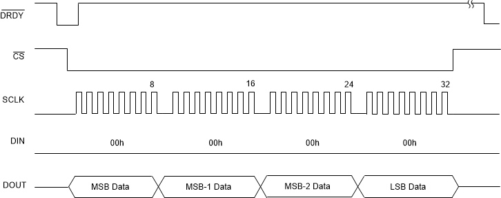
Read data direct does not require a command, instead after DRDY falls low, simply apply SCLK to read the data. Figure 7-24 shows the read data direct operation. When DRDY falls low, take CS low to start the read operation. CS low causes DOUT to transition from tri-state mode to the output of the data MSB. Data are read on the rising edge of SCLK and updated on the falling edge of SCLK. DRDY returns high on the first falling edge of SCLK. DOUT is low after 32 data bits are read. To read the same data again before new data are available, use the RDATA command.
Keep DIN low when reading conversion data. If the RDATA (read conversion data) or RREG (read register data) command is sent, output data are interrupted in response to the command. If DRDY falls low during the read operation, the new data are lost unless a minimum of three bytes of the old data are read.
 Figure 7-24 Read Data
Direct