ZHCS158C July 2012 – January 2017 ADS1299 , ADS1299-4 , ADS1299-6
PRODUCTION DATA.
- 1 特性
- 2 应用
- 3 说明
- 4 修订历史记录
- 5 Device Comparison
- 6 Pin Configuration and Functions
- 7 Specifications
- 8 Parametric Measurement Information
-
9 Detailed Description
- 9.1 Overview
- 9.2 Functional Block Diagram
- 9.3
Feature Description
- 9.3.1 Analog Functionality
- 9.3.2
Digital Functionality
- 9.3.2.1 Digital Decimation Filter
- 9.3.2.2 Clock
- 9.3.2.3 GPIO
- 9.3.2.4 ECG and EEG Specific Features
- 9.4 Device Functional Modes
- 9.5
Programming
- 9.5.1 Data Format
- 9.5.2 SPI Interface
- 9.5.3
SPI Command Definitions
- 9.5.3.1 Sending Multi-Byte Commands
- 9.5.3.2 WAKEUP: Exit STANDBY Mode
- 9.5.3.3 STANDBY: Enter STANDBY Mode
- 9.5.3.4 RESET: Reset Registers to Default Values
- 9.5.3.5 START: Start Conversions
- 9.5.3.6 STOP: Stop Conversions
- 9.5.3.7 RDATAC: Read Data Continuous
- 9.5.3.8 SDATAC: Stop Read Data Continuous
- 9.5.3.9 RDATA: Read Data
- 9.5.3.10 RREG: Read From Register
- 9.5.3.11 WREG: Write to Register
- 9.6
Register Maps
- 9.6.1
User Register Description
- 9.6.1.1 ID: ID Control Register (address = 00h) (reset = xxh)
- 9.6.1.2 CONFIG1: Configuration Register 1 (address = 01h) (reset = 96h)
- 9.6.1.3 CONFIG2: Configuration Register 2 (address = 02h) (reset = C0h)
- 9.6.1.4 CONFIG3: Configuration Register 3 (address = 03h) (reset = 60h)
- 9.6.1.5 LOFF: Lead-Off Control Register (address = 04h) (reset = 00h)
- 9.6.1.6 CHnSET: Individual Channel Settings (n = 1 to 8) (address = 05h to 0Ch) (reset = 61h)
- 9.6.1.7 BIAS_SENSP: Bias Drive Positive Derivation Register (address = 0Dh) (reset = 00h)
- 9.6.1.8 BIAS_SENSN: Bias Drive Negative Derivation Register (address = 0Eh) (reset = 00h)
- 9.6.1.9 LOFF_SENSP: Positive Signal Lead-Off Detection Register (address = 0Fh) (reset = 00h)
- 9.6.1.10 LOFF_SENSN: Negative Signal Lead-Off Detection Register (address = 10h) (reset = 00h)
- 9.6.1.11 LOFF_FLIP: Lead-Off Flip Register (address = 11h) (reset = 00h)
- 9.6.1.12 LOFF_STATP: Lead-Off Positive Signal Status Register (address = 12h) (reset = 00h)
- 9.6.1.13 LOFF_STATN: Lead-Off Negative Signal Status Register (address = 13h) (reset = 00h)
- 9.6.1.14 GPIO: General-Purpose I/O Register (address = 14h) (reset = 0Fh)
- 9.6.1.15 MISC1: Miscellaneous 1 Register (address = 15h) (reset = 00h)
- 9.6.1.16 MISC2: Miscellaneous 2 (address = 16h) (reset = 00h)
- 9.6.1.17 CONFIG4: Configuration Register 4 (address = 17h) (reset = 00h)
- 9.6.1
User Register Description
- 10Applications and Implementation
- 11Power Supply Recommendations
- 12Layout
- 13器件和文档支持
- 14机械、封装和可订购信息
10 Applications and Implementation
NOTE
Information in the following applications sections is not part of the TI component specification, and TI does not warrant its accuracy or completeness. TI’s customers are responsible for determining suitability of components for their purposes. Customers should validate and test their design implementation to confirm system functionality.
10.1 Application Information
10.1.1 Unused Inputs and Outputs
Power down unused analog inputs and connect them directly to AVDD.
Power down the Bias amplifier if unused and float BIASOUT and BIASINV. BIASIN can also float or can be tied directly to AVSS if unused.
Tie BIASREF directly to AVSS or leave floating if unused.
Tie SRB1 and SRB2 directly to AVSS or leave them floating if unused.
Do not float unused digital inputs because excessive power-supply leakage current might result. Set the two-state mode setting pins high to DVDD or low to DGND through ≥10-kΩ resistors.
Pull DRDY to supply using weak pullup resistor if unused.
If not daisy-chaining devices, tie DAISYIN directly to DGND.
10.1.2 Setting the Device for Basic Data Capture
Figure 67 outlines the procedure to configure the device in a basic state and capture data. This procedure puts the device into a configuration that matches the parameters listed in the specifications section, in order to check if the device is working properly in the user system. Follow this procedure initially until familiar with the device settings. After this procedure has been verified, the device can be configured as needed. For details on the timings for commands, see the appropriate sections in the data sheet. Sample programming codes are added for the ECG and EEG-specific functions.
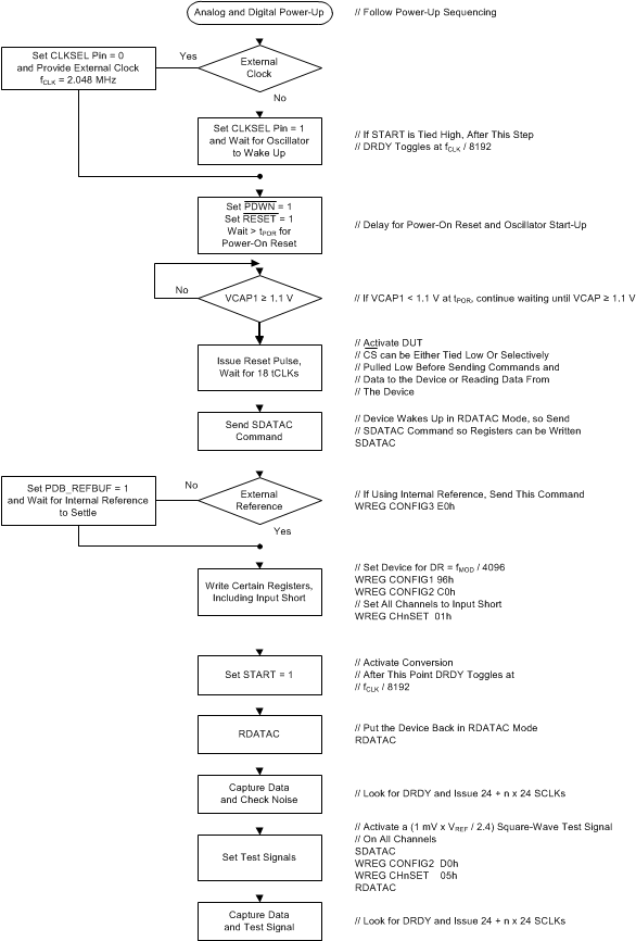 Figure 67. Initial Flow at Power-Up
10.1.2.1 Lead-Off
Sample code to set dc lead-off with pull-up and pull-down resistors on all channels.
WREG LOFF       0x13        // Comparator threshold at 95% and 5%, pullup or pulldown resistor
                            // dc lead-off
WREG CONFIG4    0x02        // Turn on dc lead-off comparators
WREG LOFF_SENSP 0xFF        // Turn on the P-side of all channels for lead-off sensing
WREG LOFF_SENSN 0xFF        // Turn on the N-side of all channels for lead-off sensing
Observe the status bits of the output data stream to monitor lead-off status.
10.1.2.2 Bias Drive
Sample code to choose bias as an average of the first three channels.
WREG RLD_SENSP 0x07        // Select channel 1-3 P-side for RLD sensing
WREG RLD_SENSN 0x07        // Select channel 1-3 N-side for RLD sensing
WREG CONFIG3   b’x1xx 1100 // Turn on BIAS amplifier, set internal BIASREF voltage
Sample code to route the BIASOUT signal through channel 4 N-side and measure bias with channel 5. Make sure the external side to the chip BIASOUT is connected to BIASIN.
WREG CONFIG3 b’xxx1 1100  // Turn on BIAS amp, set internal BIASREF voltage, set BIAS measurement bit
WREG CH4SET  b’xxxx 0111  // Route BIASIN to channel 4 N-side
WREG CH5SET  b’xxxx 0010  // Route BIASIN to be measured at channel 5 w.r.t BIASREF
10.1.3 Establishing the Input Common-Mode
The ADS1299-x measures fully-differential signals where the common-mode voltage point is the midpoint of the positive and negative analog input. The internal PGA restricts the common-mode input range because of the headroom required for operation. The human body is prone to common-mode drifts because noise easily couples onto the human body, similar to an antenna. These common-mode drifts may push the ADS1299-x input common-mode voltage out of the measurable range of the ADC.
If a patient-drive electrode is used by the system, the ADS1299-x includes an on-chip bias drive (BIAS) amplifier that connects to the patient drive electrode. The BIAS amplifier function is to bias the patient to maintain the other electrode common-mode voltages within the valid range. When powered on, the amplifier uses either the analog midsupply voltage, or the voltage present at the BIASREF pin, as a reference input to drive the patient to that voltage.
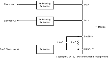
The ADS1299-x provides the option to use input electrode voltages as feedback to the amplifier to more effectively stabilize the output to the amplifier reference voltage by setting corresponding bits in the BIAS_SENSP and BIAS_SENSN registers. Figure 68 shows an example of a three-electrode system that leverages this technique.
10.1.4 Multiple Device Configuration
The ADS1299-x is designed to provide configuration flexibility when multiple devices are used in a system. The serial interface typically needs four signals: DIN, DOUT, SCLK, and CS. With one additional chip select signal per device, multiple devices can be connected together. The number of signals needed to interface n devices is 3 + n.
The BIAS drive amplifiers can be daisy-chained, as explained in the Bias Configuration with Multiple Devices section. To use the internal oscillator in a daisy-chain configuration, one device must be set as the master for the clock source with the internal oscillator enabled (CLKSEL pin = 1) and the internal oscillator clock brought out of the device by setting the CLK_EN register bit to '1'. This master device clock is used as the external clock source for other devices.
When using multiple devices, the devices can be synchronized with the START signal. The delay from START to the DRDY signal is fixed for a given data rate (see the Start subsection of the SPI Interface section for more details on the settling times). Figure 69 shows the behavior of two devices when synchronized with the START signal.
There are two ways to connect multiple devices with a optimal number of interface pins: cascade mode and daisy-chain mode.
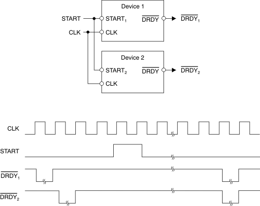 Figure 69. Synchronizing Multiple Converters
10.1.4.1 Cascaded Mode
Figure 70a illustrates a configuration with two devices cascaded together. Together, the devices create a system with 16 channels. DOUT, SCLK, and DIN are shared. Each device has its own chip select. When a device is not selected by the corresponding CS being driven to logic 1, the DOUT of this device is high-impedance. This structure allows the other device to take control of the DOUT bus. This configuration method is suitable for the majority of applications.
10.1.4.2 Daisy-Chain Mode
Daisy-chain mode is enabled by setting the DAISY_EN bit in the CONFIG1 register. Figure 70b shows the daisy-chain configuration. In this mode SCLK, DIN, and CS are shared across multiple devices. The DOUT of the second device is connected to the DAISY_IN of the first device, thereby creating a chain. When using daisy-chain mode, the multiple readback feature is not available. Short the DAISY_IN pin to digital ground if not used. Figure 2 describes the required timing for the device shown in the configurations of Figure 70. Status and data from device 1 appear first on DOUT, followed by the status and data from device 2. The ADS1299 can be daisy chained with a second ADS1299, an ADS1299-6, or an ADS1299-4.
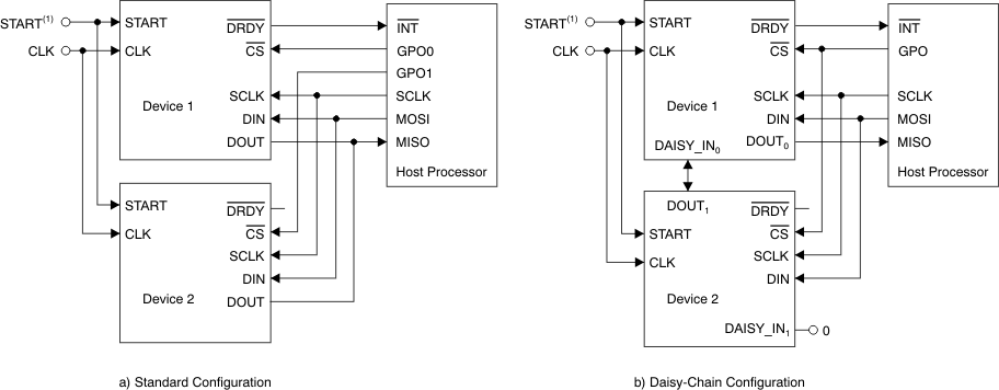
When all devices in the chain operate in the same register setting, DIN can be shared as well. This configuration reduces the SPI communication signals to four, regardless of the number of devices. The BIAS driver cannot be shared among the multiple devices and an external clock must be used because the individual devices cannot be programmed when sharing a common DIN.
Note that from Figure 2, the SCLK rising edge shifts data out of the device on DOUT. The SCLK negative edge is used to latch data into the device DAISY_IN pin down the chain. This architecture allows for a faster SCLK rate speed, but also makes the interface sensitive to board-level signal delays. The more devices in the chain, the more challenging adhering to setup and hold times becomes. A star-pattern connection of SCLK to all devices, minimizing DOUT length, and other printed circuit board (PCB) layout techniques helps. Placing delay circuits (such as buffers) between DOUT and DAISY_IN are ways to mitigate this challenge. One other option is to insert a D flip-flop between DOUT and DAISY_IN clocked on an inverted SCLK. Note also that daisy-chain mode requires some software overhead to recombine data bits spread across byte boundaries. Figure 71 shows a timing diagram for this mode.
 Figure 71. Daisy-Chain Timing
The maximum number of devices that can be daisy-chained depends on the data rate at which the device is operated at. The maximum number of devices can be approximately calculated with Equation 10.

where
For example, when the 8-channel ADS1299 is operated at a 2-kSPS data rate with a 4-MHz fSCLK, 10 devices can be daisy-chained.
10.2 Typical Application
The biopotential signals that are measured in electroencephalography (EEG) are small when compared to other types of biopotential signals. The ADS1299 is equipped to measure such small signals due to its extremely low input-referred noise from its high performance internal PGA. Figure 72 and Figure 73 are examples of how the ADS1299 may be configured in typical EEG measurement setups. Figure 72 shows how to measure electrode potentials in a sequential montage, whereas Figure 73 illustrates referential montage measurement connections.
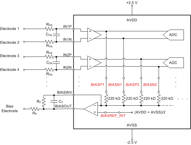 Figure 72. Example Schematic Using the ADS1299 in an EEG Data Acquisition Application, Sequential Montage
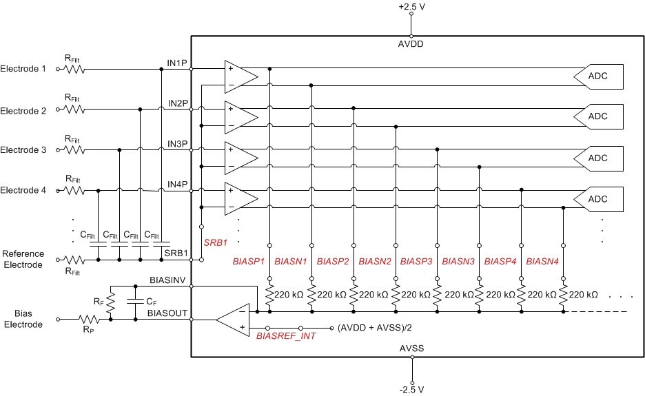 Figure 73. Example Schematic Using the ADS1299 in an EEG Data Acquisition Application, Referential Montage
10.2.1 Design Requirements
Table 29 shows the design requirements for a typical EEG measurement system.
Table 29. EEG Data Acquisition Design Requirements
| DESIGN PARAMETER | VALUE |
|---|---|
| Bandwidth | 1 Hz - 50 Hz |
| Minimum signal bandwidth | 10 μVPk |
| Input Impedance | > 10 MΩ |
| Coupling | dc |
10.2.2 Detailed Design Procedure
Each channel on the ADS1299 is optimized to measure a separate EEG waveform. The specific connections depend on the EEG montage. The sequential montage is a configuration where each channel represents the voltage between two adjacent electrodes. For example, to measure the potential between electrode Fp1 and F7 on channel 1 of the ADS1299, route the Fp1 electrode to IN1P and the F7 electrode to IN1N. The connections for a sequential montage are illustrated in Figure 72.
Alternatively, EEG electrodes can be measured in a referential montage in which each of the electrodes is measured with respect to a single reference electrode. This montage also allows calculation of the waveforms that would have been measured in a sequential montage by finding the difference between two electrode waveforms which were measured with respect to the same electrode. The ADS1299 allows for such a configuration through the use of the SRB1 pin. The SRB1 pin on the ADS1299 may be internally routed to each channel negative input by setting the SRB1 bit in the MISC1 register. When the reference electrode is connected to the SRB1 pin and all other electrodes are connected to the respective positive channel inputs, the electrode voltages can be measured with a referential montage. The referential montage is illustrated in Figure 73. See Figure 18 for a diagram of the channel input multiplexer options.
The ADS1299 is designed to be an EEG front end such that no additional amplification or buffer stage is needed between the electrodes and ADS1299. The ADS1299 has a low-noise PGA with excellent input-referred noise performance. For certain data rate and gain settings, the ADS1299 introduces significantly less than 1 μVRMS of input-referred noise to the signal chain making the device more than capable of handling the 10-μVPk minimum signal amplitude. ADS1299 noise performance for different PGA gains and data rate settings is listed in Table 1, Table 2, Table 3, and Table 4.
Traditional EEG data acquisition systems high-pass filter the signals in the front-end to remove dc signal content. This topology allows the signal to be amplified by a large gain so the signal can be digitized by a 12- to 16-bit ADC. The ADS1299 24-bit resolution allows the signal to be dc-coupled to the ADC because small EEG signal information can be measured in addition to a significant dc offset.
The ADS1299 channel inputs have very low input bias current allowing electrodes to be connected to the inputs of the ADS1299 with very little leakage current flowing on the patient cables. The ADS1299 has a minimum dc input impedance of 1 GΩ when the lead-off current sources are disabled and 500 MΩ typically when the lead-off current sources are enabled.
The passive components RFilt and CFilt form low-pass filters. In general, the filter is advised to be formed by using a differential capacitor CFIlt that shunts the inputs rather than individual RC filters whose capacitors shunt to ground. The differential capacitor configuration significantly improves common-mode rejection because this approach removes dependence on component mismatch.
The cutoff frequency for the filter can be placed well past the data rate of the ADC because of the delta-sigma ADC filter-then-decimate topology. Take care to prevent aliasing around the first repetition of the digital decimation filter response at fMOD. Assuming a 2.048-MHz fCLK, fMOD = 1.024 MHz. The value of RFilt has a minimum set by technical standards for medical electronics. The capacitor value must be set to arrange the proper cutoff frequency.
If the system is likely to be exposed to high-frequency EMI, adding very small-value, common-mode capacitors to the inputs is advisable to filter high-frequency common-mode signals. If these capacitors are added, then the capacitors should be 10 or 20 times smaller than the differential capacitor to ensure their effect of CMRR is minimized.
The integrated bias amplifier serves two purposes in an EEG data acquisition system with the ADS1299. The bias amplifier provides a bias voltage that, when applied to the patient, keeps the measurement electrode common-mode voltage within the rails of the ADS1299. This scenario allows for dc coupling. In addition, the bias amplifier can be configured to provide negative common-mode feedback to the patient to cancel unwanted common-mode signals appearing on the electrodes. This feature is especially helpful because biopotential acquisition systems are notoriously prone to mains-frequency common-mode interference.
The bias amplifier is powered on by setting the PD_BIAS bit in the CONFIG3 register. Set the BIASREF_INT bit in the CONFIG3 register to input the internally generated analog mid-supply voltage the noninverting input of the bias amplifier. To enable an electrode as an input to the bias amplifier, set the corresponding bit in the BIAS_SENSP or BIAS_SENSN register.
The dc gain of the bias amplifier is determined by RBias and the number of channel inputs enabled as inputs to the bias amplifier. The bias amplifier circuit only passes common-mode signals. Therefore, the 330-kΩ resistors at each PGA output are in parallel for common-mode signals. The bias amplifier is configured in an inverting gain scheme. The formula for determining dc gain for common-mode signals input to the bias amplifier is shown in Equation 11. The capacitor Cf sets the bandwidth for the bias amplifier. Ensure that the amplifier has enough bandwidth to output all the intended common-mode signals.

Another advantage to a dc-coupled EEG data acquisition system is the ability to detect when an electrode no longer makes good contact with the patient. The ADS1299 features integrated lead-off detection electronics. The Lead-Off Detection section explains how to use the lead-off feature on the ADS1299. Note that when configured in a referential montage, only use one lead-off current source with the reference electrode.
10.2.3 Application Curves
Testing the capability of the ADS1299 to measure signals in the band and near the amplitude of typical EEG signals can be done with a precision signal generator. The ADS1299 was tested in a configuration like the one shown in Figure 74.
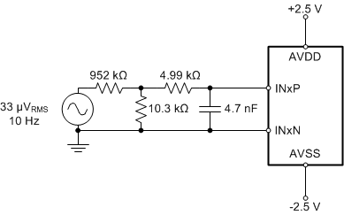 Figure 74. Example Schematic Using the ADS1299 in an EEG Data Acquisition Application, Referential Montage
The 952-kΩ and 10.3-kΩ resistors were used to attenuate the voltage from the signal source because the source could not reach the desired magnitude directly. With the voltage divider, the signal appearing at the inputs was a 3.5-μVRMS, 10-Hz sine wave. Figure 75 shows the input-referred conversion results from the ADS1299 following calibration for offset. The signal that is measured is similar to some of the smallest extracranial EEG signals that can be measured with typical EEG acquisition systems. The signal can be clearly identified. Given this measurement setup was a single-ended configuration without shielding, the measurement setup was subject to significant mains interference. A digital low-pass filter was applied to remove the interference.
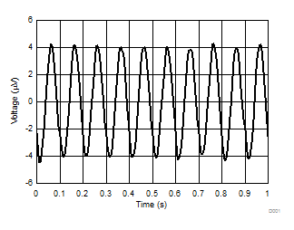 Figure 75. ADS1299 10-Hz Input Signal Results
