ZHCSEV8D March 2016 – January 2018 ADS131A02 , ADS131A04
PRODUCTION DATA.
- 1 特性
- 2 应用
- 3 说明
- 4 修订历史记录
- 5 Device Comparison Table
- 6 Pin Configuration and Functions
-
7 Specifications
- 7.1 Absolute Maximum Ratings
- 7.2 ESD Ratings
- 7.3 Recommended Operating Conditions
- 7.4 Thermal Information
- 7.5 Electrical Characteristics
- 7.6 Timing Requirements: Asynchronous Interrupt Interface Mode
- 7.7 Switching Characteristics: Asynchronous Interrupt Interface Mode
- 7.8 Timing Requirements: Synchronous Master Interface Mode
- 7.9 Switching Characteristics: Synchronous Master Interface Mode
- 7.10 Timing Requirements: Synchronous Slave Interface Mode
- 7.11 Switching Characteristics: Synchronous Slave Interface Mode
- 7.12 Typical Characteristics
- 8 Parameter Measurement Information
-
9 Detailed Description
- 9.1 Overview
- 9.2 Functional Block Diagram
- 9.3 Feature Description
- 9.4 Device Functional Modes
- 9.5
Programming
- 9.5.1 Interface Protocol
- 9.5.2 SPI Interface
- 9.5.3
SPI Command Definitions
- 9.5.3.1 NULL: Null Command
- 9.5.3.2 RESET: Reset to POR Values
- 9.5.3.3 STANDBY: Enter Standby Mode
- 9.5.3.4 WAKEUP: Exit STANDBY Mode
- 9.5.3.5 LOCK: Lock ADC Registers
- 9.5.3.6 UNLOCK: Unlock ADC Registers
- 9.5.3.7 RREG: Read a Single Register
- 9.5.3.8 RREGS: Read Multiple Registers
- 9.5.3.9 WREG: Write Single Register
- 9.5.3.10 WREGS: Write Multiple Registers
- 9.6
Register Maps
- 9.6.1
User Register Description
- 9.6.1.1 ID_MSB: ID Control Register MSB (address = 00h) [reset = xxh]
- 9.6.1.2 ID_LSB: ID Control Register LSB (address = 01h) [reset = xxh]
- 9.6.1.3 STAT_1: Status 1 Register (address = 02h) [reset = 00h]
- 9.6.1.4 STAT_P: Positive Input Fault Detect Status Register (address = 03h) [reset = 00h]
- 9.6.1.5 STAT_N: Negative Input Fault Detect Status Register (address = 04h) [reset = 00h]
- 9.6.1.6 STAT_S: SPI Status Register (address = 05h) [reset = 00h]
- 9.6.1.7 ERROR_CNT: Error Count Register (address = 06h) [reset = 00h]
- 9.6.1.8 STAT_M2: Hardware Mode Pin Status Register (address = 07h) [reset = xxh]
- 9.6.1.9 Reserved Registers (address = 08h to 0Ah) [reset = 00h]
- 9.6.1.10 A_SYS_CFG: Analog System Configuration Register (address = 0Bh) [reset = 60h]
- 9.6.1.11 D_SYS_CFG: Digital System Configuration Register (address = 0Ch) [reset = 3Ch]
- 9.6.1.12 CLK1: Clock Configuration 1 Register (address = 0Dh) [reset = 08h]
- 9.6.1.13 CLK2: Clock Configuration 2 Register (address = 0Eh) [reset = 86h]
- 9.6.1.14 ADC_ENA: ADC Channel Enable Register (address = 0Fh) [reset = 00h]
- 9.6.1.15 Reserved Register (address = 10h) [reset = 00h]
- 9.6.2 ADCx: ADC Channel Digital Gain Configuration Registers (address = 11h to 14h) [reset = 00h]
- 9.6.1
User Register Description
- 10Application and Implementation
- 11Power Supply Recommendations
- 12Layout
- 13器件和文档支持
- 14机械、封装和可订购信息
10.1.2 Power Monitoring Specific Applications
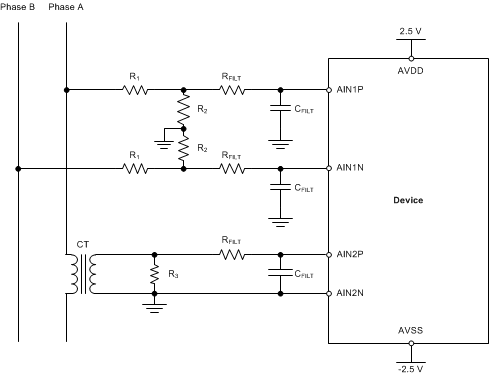
Each channel of the ADS131A0x is identical, giving designers the flexibility to sense voltage or current with any channel. Simultaneous sampling allows the application to calculate instantaneous power for any simultaneous voltage and current measurement. Figure 95 shows an example system that measures voltage and current simultaneously.
 Figure 95. Example Power-Monitoring System
In Figure 95, channel 1 is dedicated to measuring the voltage between phase A and phase B and channel 2 is dedicated to measuring the current on phase A.
The resistors R1 and R2 form a voltage divider that steps the line voltage down to within the measurement range of the ADC. R1 can be formed by multiple resistors in series to dissipate power across several components. This configuration is also valid if the voltage is measured with respect to neutral instead of between phases.
Channel 2 is dedicated to measuring current that flows on phase A. Resistor R3 serves as a burden resistor that shunts the current flowing across the secondary coil of the current transformer (CT). Current can also be measured using a Rogowski coil and an analog integrator or by performing integration digitally after a conversion.
The RC filters formed by RFILT and CFILT serve as antialiasing filters for the converter. If an application requires a steeper filter roll-off, a second-order RC filter can be used.