ZHCSEV8D March   2016  – January 2018 ADS131A02 , ADS131A04

PRODUCTION DATA.  

  1. 特性
  2. 应用
  3. 说明
    1.     简化框图
  4. 修订历史记录
  5. Device Comparison Table
  6. Pin Configuration and Functions
    1.     Pin Functions
  7. Specifications
    1. 7.1  Absolute Maximum Ratings
    2. 7.2  ESD Ratings
    3. 7.3  Recommended Operating Conditions
    4. 7.4  Thermal Information
    5. 7.5  Electrical Characteristics
    6. 7.6  Timing Requirements: Asynchronous Interrupt Interface Mode
    7. 7.7  Switching Characteristics: Asynchronous Interrupt Interface Mode
    8. 7.8  Timing Requirements: Synchronous Master Interface Mode
    9. 7.9  Switching Characteristics: Synchronous Master Interface Mode
    10. 7.10 Timing Requirements: Synchronous Slave Interface Mode
    11. 7.11 Switching Characteristics: Synchronous Slave Interface Mode
    12. 7.12 Typical Characteristics
  8. Parameter Measurement Information
    1. 8.1 Noise Measurements
  9. Detailed Description
    1. 9.1 Overview
    2. 9.2 Functional Block Diagram
    3. 9.3 Feature Description
      1. 9.3.1 Clock
        1. 9.3.1.1 XTAL1/CLKIN and XTAL2
        2. 9.3.1.2 ICLK
        3. 9.3.1.3 MODCLK
        4. 9.3.1.4 Data Rate
      2. 9.3.2 Analog Input
      3. 9.3.3 Input Overrange and Underrange Detection
      4. 9.3.4 Reference
      5. 9.3.5 ΔΣ Modulator
      6. 9.3.6 Digital Decimation Filter
      7. 9.3.7 Watchdog Timer
    4. 9.4 Device Functional Modes
      1. 9.4.1 Low-Power and High-Resolution Mode
      2. 9.4.2 Power-Up
      3. 9.4.3 Standby and Wake-Up Mode
      4. 9.4.4 Conversion Mode
      5. 9.4.5 Reset (RESET)
    5. 9.5 Programming
      1. 9.5.1 Interface Protocol
        1. 9.5.1.1 Device Word Length
        2. 9.5.1.2 Fixed versus Dynamic-Frame Mode
        3. 9.5.1.3 Command Word
        4. 9.5.1.4 Status Word
        5. 9.5.1.5 Data Words
        6. 9.5.1.6 Cyclic Redundancy Check (CRC)
          1. 9.5.1.6.1 Computing the CRC
        7. 9.5.1.7 Hamming Code Error Correction
      2. 9.5.2 SPI Interface
        1. 9.5.2.1 Asynchronous Interrupt Mode
          1. 9.5.2.1.1 Chip Select (CS)
          2. 9.5.2.1.2 Serial Clock (SCLK)
          3. 9.5.2.1.3 Data Input (DIN)
          4. 9.5.2.1.4 Data Output (DOUT)
          5. 9.5.2.1.5 Data Ready (DRDY)
          6. 9.5.2.1.6 Asynchronous Interrupt Mode Data Retrieval
        2. 9.5.2.2 Synchronous Master Mode
          1. 9.5.2.2.1 Serial Clock (SCLK)
          2. 9.5.2.2.2 Data Input (DIN)
          3. 9.5.2.2.3 Data Output (DOUT)
          4. 9.5.2.2.4 Data Ready (DRDY)
          5. 9.5.2.2.5 Chip Select (CS)
          6. 9.5.2.2.6 Synchronous Master Mode Data Retrieval
        3. 9.5.2.3 Synchronous Slave Mode
          1. 9.5.2.3.1 Chip Select (CS)
          2. 9.5.2.3.2 Serial Clock (SCLK)
          3. 9.5.2.3.3 Data Input (DIN)
          4. 9.5.2.3.4 Data Output (DOUT)
          5. 9.5.2.3.5 Data Ready (DRDY)
          6. 9.5.2.3.6 Synchronous Slave Mode Data Retrieval
        4. 9.5.2.4 ADC Frame Complete (DONE)
      3. 9.5.3 SPI Command Definitions
        1. 9.5.3.1  NULL: Null Command
        2. 9.5.3.2  RESET: Reset to POR Values
        3. 9.5.3.3  STANDBY: Enter Standby Mode
        4. 9.5.3.4  WAKEUP: Exit STANDBY Mode
        5. 9.5.3.5  LOCK: Lock ADC Registers
        6. 9.5.3.6  UNLOCK: Unlock ADC Registers
          1. 9.5.3.6.1 UNLOCK from POR or RESET
        7. 9.5.3.7  RREG: Read a Single Register
        8. 9.5.3.8  RREGS: Read Multiple Registers
        9. 9.5.3.9  WREG: Write Single Register
        10. 9.5.3.10 WREGS: Write Multiple Registers
    6. 9.6 Register Maps
      1. 9.6.1 User Register Description
        1. 9.6.1.1  ID_MSB: ID Control Register MSB (address = 00h) [reset = xxh]
          1. Table 16. ID_MSB Register Field Descriptions
        2. 9.6.1.2  ID_LSB: ID Control Register LSB (address = 01h) [reset = xxh]
          1. Table 17. ID_LSB Register Field Descriptions
        3. 9.6.1.3  STAT_1: Status 1 Register (address = 02h) [reset = 00h]
          1. Table 18. STAT_1 Register Field Descriptions
        4. 9.6.1.4  STAT_P: Positive Input Fault Detect Status Register (address = 03h) [reset = 00h]
          1. Table 19. STAT_P Register Field Descriptions
        5. 9.6.1.5  STAT_N: Negative Input Fault Detect Status Register (address = 04h) [reset = 00h]
          1. Table 20. STAT_N Register Field Descriptions
        6. 9.6.1.6  STAT_S: SPI Status Register (address = 05h) [reset = 00h]
          1. Table 21. STAT_S Register Field Descriptions
        7. 9.6.1.7  ERROR_CNT: Error Count Register (address = 06h) [reset = 00h]
          1. Table 22. ERROR_CNT Register Field Descriptions
        8. 9.6.1.8  STAT_M2: Hardware Mode Pin Status Register (address = 07h) [reset = xxh]
          1. Table 23. STAT_M2 Register Field Descriptions
        9. 9.6.1.9  Reserved Registers (address = 08h to 0Ah) [reset = 00h]
          1. Table 24. Reserved Registers Field Descriptions
        10. 9.6.1.10 A_SYS_CFG: Analog System Configuration Register (address = 0Bh) [reset = 60h]
          1. Table 25. A_SYS_CFG Register Field Descriptions
        11. 9.6.1.11 D_SYS_CFG: Digital System Configuration Register (address = 0Ch) [reset = 3Ch]
          1. Table 27. D_SYS_CFG Register Field Descriptions
        12. 9.6.1.12 CLK1: Clock Configuration 1 Register (address = 0Dh) [reset = 08h]
          1. Table 28. CLK1 Register Field Descriptions
        13. 9.6.1.13 CLK2: Clock Configuration 2 Register (address = 0Eh) [reset = 86h]
          1. Table 29. CLK2 Register Field Descriptions
        14. 9.6.1.14 ADC_ENA: ADC Channel Enable Register (address = 0Fh) [reset = 00h]
          1. Table 31. ADC_ENA Register Field Descriptions
        15. 9.6.1.15 Reserved Register (address = 10h) [reset = 00h]
          1. Table 32. Reserved Register Field Descriptions
      2. 9.6.2 ADCx: ADC Channel Digital Gain Configuration Registers (address = 11h to 14h) [reset = 00h]
        1. Table 33. ADCx Registers Field Descriptions
  10. 10Application and Implementation
    1. 10.1 Application Information
      1. 10.1.1 Unused Inputs and Outputs
      2. 10.1.2 Power Monitoring Specific Applications
      3. 10.1.3 Multiple Device Configuration
        1. 10.1.3.1 First Device Configured in Asynchronous Interrupt Mode
        2. 10.1.3.2 First Device Configured in Synchronous Master Mode
        3. 10.1.3.3 All Devices Configured in Synchronous Slave Mode
    2. 10.2 Typical Application
      1. 10.2.1 Design Requirements
      2. 10.2.2 Detailed Design Procedure
      3. 10.2.3 Application Curve
    3. 10.3 Do's and Don'ts
    4. 10.4 Initialization Set Up
  11. 11Power Supply Recommendations
    1. 11.1 Negative Charge Pump
    2. 11.2 Internal Digital LDO
    3. 11.3 Power-Supply Sequencing
    4. 11.4 Power-Supply Decoupling
  12. 12Layout
    1. 12.1 Layout Guidelines
    2. 12.2 Layout Example
  13. 13器件和文档支持
    1. 13.1 文档支持
      1. 13.1.1 相关文档
    2. 13.2 相关链接
    3. 13.3 接收文档更新通知
    4. 13.4 社区资源
    5. 13.5 商标
    6. 13.6 静电放电警告
    7. 13.7 Glossary
  14. 14机械、封装和可订购信息

封装选项

机械数据 (封装 | 引脚)
散热焊盘机械数据 (封装 | 引脚)
订购信息

All Devices Configured in Synchronous Slave Mode

Figure 100 illustrates a multiple device configuration where all devices are configured in synchronous slave mode. Figure 100 illustrates an external clock at the CLKIN pin, but a free-running SCLK can also be used as the conversion clock in this mode. SCLK must be free-running if the modulator clock is derived from the serial clock (CLKSRC = 1). See the Synchronous Slave Mode section for more information about clocking the device using SCLK. The DONE pin of each device connects to the CS pin of the subsequent device for communication. The DOUT pin of a device whose contents are already shifted out assumes a high-impedance state, allowing the DOUT pins of all devices to be tied together. To send commands to specific devices, send the respective command to the device when that device is selected for communication. In this configuration, conversions must be synchronized by the master. Synchronization is accomplished by tying the chip select or frame sync output of the host to the DRDY input of each device. See the Synchronous Slave Mode section for more information about conversion synchronization using slave mode. Figure 101 illustrates an example interface timing diagram for this configuration.
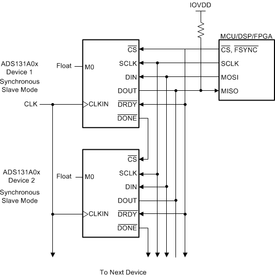
ADS131A02 ADS131A04 apps_syncS_chain_sbas590.gifFigure 100. Multiple Device Configuration Using Synchronous Slave Mode
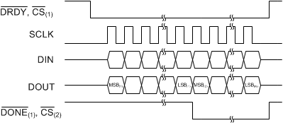
ADS131A02 ADS131A04 apps_syncS_chain_timing_sbas590.gif

NOTE:

(1) denotes device 1, (2) denotes device 2, and (N) denotes device N.
Figure 101. Multiple Device Configuration Timing Diagram When Using Synchronous Slave Mode