ZHCSEV8D March   2016  – January 2018 ADS131A02 , ADS131A04

PRODUCTION DATA.  

  1. 特性
  2. 应用
  3. 说明
    1.     简化框图
  4. 修订历史记录
  5. Device Comparison Table
  6. Pin Configuration and Functions
    1.     Pin Functions
  7. Specifications
    1. 7.1  Absolute Maximum Ratings
    2. 7.2  ESD Ratings
    3. 7.3  Recommended Operating Conditions
    4. 7.4  Thermal Information
    5. 7.5  Electrical Characteristics
    6. 7.6  Timing Requirements: Asynchronous Interrupt Interface Mode
    7. 7.7  Switching Characteristics: Asynchronous Interrupt Interface Mode
    8. 7.8  Timing Requirements: Synchronous Master Interface Mode
    9. 7.9  Switching Characteristics: Synchronous Master Interface Mode
    10. 7.10 Timing Requirements: Synchronous Slave Interface Mode
    11. 7.11 Switching Characteristics: Synchronous Slave Interface Mode
    12. 7.12 Typical Characteristics
  8. Parameter Measurement Information
    1. 8.1 Noise Measurements
  9. Detailed Description
    1. 9.1 Overview
    2. 9.2 Functional Block Diagram
    3. 9.3 Feature Description
      1. 9.3.1 Clock
        1. 9.3.1.1 XTAL1/CLKIN and XTAL2
        2. 9.3.1.2 ICLK
        3. 9.3.1.3 MODCLK
        4. 9.3.1.4 Data Rate
      2. 9.3.2 Analog Input
      3. 9.3.3 Input Overrange and Underrange Detection
      4. 9.3.4 Reference
      5. 9.3.5 ΔΣ Modulator
      6. 9.3.6 Digital Decimation Filter
      7. 9.3.7 Watchdog Timer
    4. 9.4 Device Functional Modes
      1. 9.4.1 Low-Power and High-Resolution Mode
      2. 9.4.2 Power-Up
      3. 9.4.3 Standby and Wake-Up Mode
      4. 9.4.4 Conversion Mode
      5. 9.4.5 Reset (RESET)
    5. 9.5 Programming
      1. 9.5.1 Interface Protocol
        1. 9.5.1.1 Device Word Length
        2. 9.5.1.2 Fixed versus Dynamic-Frame Mode
        3. 9.5.1.3 Command Word
        4. 9.5.1.4 Status Word
        5. 9.5.1.5 Data Words
        6. 9.5.1.6 Cyclic Redundancy Check (CRC)
          1. 9.5.1.6.1 Computing the CRC
        7. 9.5.1.7 Hamming Code Error Correction
      2. 9.5.2 SPI Interface
        1. 9.5.2.1 Asynchronous Interrupt Mode
          1. 9.5.2.1.1 Chip Select (CS)
          2. 9.5.2.1.2 Serial Clock (SCLK)
          3. 9.5.2.1.3 Data Input (DIN)
          4. 9.5.2.1.4 Data Output (DOUT)
          5. 9.5.2.1.5 Data Ready (DRDY)
          6. 9.5.2.1.6 Asynchronous Interrupt Mode Data Retrieval
        2. 9.5.2.2 Synchronous Master Mode
          1. 9.5.2.2.1 Serial Clock (SCLK)
          2. 9.5.2.2.2 Data Input (DIN)
          3. 9.5.2.2.3 Data Output (DOUT)
          4. 9.5.2.2.4 Data Ready (DRDY)
          5. 9.5.2.2.5 Chip Select (CS)
          6. 9.5.2.2.6 Synchronous Master Mode Data Retrieval
        3. 9.5.2.3 Synchronous Slave Mode
          1. 9.5.2.3.1 Chip Select (CS)
          2. 9.5.2.3.2 Serial Clock (SCLK)
          3. 9.5.2.3.3 Data Input (DIN)
          4. 9.5.2.3.4 Data Output (DOUT)
          5. 9.5.2.3.5 Data Ready (DRDY)
          6. 9.5.2.3.6 Synchronous Slave Mode Data Retrieval
        4. 9.5.2.4 ADC Frame Complete (DONE)
      3. 9.5.3 SPI Command Definitions
        1. 9.5.3.1  NULL: Null Command
        2. 9.5.3.2  RESET: Reset to POR Values
        3. 9.5.3.3  STANDBY: Enter Standby Mode
        4. 9.5.3.4  WAKEUP: Exit STANDBY Mode
        5. 9.5.3.5  LOCK: Lock ADC Registers
        6. 9.5.3.6  UNLOCK: Unlock ADC Registers
          1. 9.5.3.6.1 UNLOCK from POR or RESET
        7. 9.5.3.7  RREG: Read a Single Register
        8. 9.5.3.8  RREGS: Read Multiple Registers
        9. 9.5.3.9  WREG: Write Single Register
        10. 9.5.3.10 WREGS: Write Multiple Registers
    6. 9.6 Register Maps
      1. 9.6.1 User Register Description
        1. 9.6.1.1  ID_MSB: ID Control Register MSB (address = 00h) [reset = xxh]
          1. Table 16. ID_MSB Register Field Descriptions
        2. 9.6.1.2  ID_LSB: ID Control Register LSB (address = 01h) [reset = xxh]
          1. Table 17. ID_LSB Register Field Descriptions
        3. 9.6.1.3  STAT_1: Status 1 Register (address = 02h) [reset = 00h]
          1. Table 18. STAT_1 Register Field Descriptions
        4. 9.6.1.4  STAT_P: Positive Input Fault Detect Status Register (address = 03h) [reset = 00h]
          1. Table 19. STAT_P Register Field Descriptions
        5. 9.6.1.5  STAT_N: Negative Input Fault Detect Status Register (address = 04h) [reset = 00h]
          1. Table 20. STAT_N Register Field Descriptions
        6. 9.6.1.6  STAT_S: SPI Status Register (address = 05h) [reset = 00h]
          1. Table 21. STAT_S Register Field Descriptions
        7. 9.6.1.7  ERROR_CNT: Error Count Register (address = 06h) [reset = 00h]
          1. Table 22. ERROR_CNT Register Field Descriptions
        8. 9.6.1.8  STAT_M2: Hardware Mode Pin Status Register (address = 07h) [reset = xxh]
          1. Table 23. STAT_M2 Register Field Descriptions
        9. 9.6.1.9  Reserved Registers (address = 08h to 0Ah) [reset = 00h]
          1. Table 24. Reserved Registers Field Descriptions
        10. 9.6.1.10 A_SYS_CFG: Analog System Configuration Register (address = 0Bh) [reset = 60h]
          1. Table 25. A_SYS_CFG Register Field Descriptions
        11. 9.6.1.11 D_SYS_CFG: Digital System Configuration Register (address = 0Ch) [reset = 3Ch]
          1. Table 27. D_SYS_CFG Register Field Descriptions
        12. 9.6.1.12 CLK1: Clock Configuration 1 Register (address = 0Dh) [reset = 08h]
          1. Table 28. CLK1 Register Field Descriptions
        13. 9.6.1.13 CLK2: Clock Configuration 2 Register (address = 0Eh) [reset = 86h]
          1. Table 29. CLK2 Register Field Descriptions
        14. 9.6.1.14 ADC_ENA: ADC Channel Enable Register (address = 0Fh) [reset = 00h]
          1. Table 31. ADC_ENA Register Field Descriptions
        15. 9.6.1.15 Reserved Register (address = 10h) [reset = 00h]
          1. Table 32. Reserved Register Field Descriptions
      2. 9.6.2 ADCx: ADC Channel Digital Gain Configuration Registers (address = 11h to 14h) [reset = 00h]
        1. Table 33. ADCx Registers Field Descriptions
  10. 10Application and Implementation
    1. 10.1 Application Information
      1. 10.1.1 Unused Inputs and Outputs
      2. 10.1.2 Power Monitoring Specific Applications
      3. 10.1.3 Multiple Device Configuration
        1. 10.1.3.1 First Device Configured in Asynchronous Interrupt Mode
        2. 10.1.3.2 First Device Configured in Synchronous Master Mode
        3. 10.1.3.3 All Devices Configured in Synchronous Slave Mode
    2. 10.2 Typical Application
      1. 10.2.1 Design Requirements
      2. 10.2.2 Detailed Design Procedure
      3. 10.2.3 Application Curve
    3. 10.3 Do's and Don'ts
    4. 10.4 Initialization Set Up
  11. 11Power Supply Recommendations
    1. 11.1 Negative Charge Pump
    2. 11.2 Internal Digital LDO
    3. 11.3 Power-Supply Sequencing
    4. 11.4 Power-Supply Decoupling
  12. 12Layout
    1. 12.1 Layout Guidelines
    2. 12.2 Layout Example
  13. 13器件和文档支持
    1. 13.1 文档支持
      1. 13.1.1 相关文档
    2. 13.2 相关链接
    3. 13.3 接收文档更新通知
    4. 13.4 社区资源
    5. 13.5 商标
    6. 13.6 静电放电警告
    7. 13.7 Glossary
  14. 14机械、封装和可订购信息

封装选项

机械数据 (封装 | 引脚)
散热焊盘机械数据 (封装 | 引脚)
订购信息

Typical Characteristics

at TA = 25°C, IOVDD = 3.3 V, AVDD = 2.5 V, AVSS = –2.5 V, VNCPEN (register 0Bh, bit 7) = 0, internal VREF = 2.442 V, fCLKIN = 16.384 MHz, fMOD = 4.096 MHz, data rate = 8 kSPS, HR mode, and gain = 1 (unless otherwise noted)
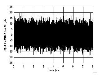
ADS131A02 ADS131A04 D008_sbas590.gif
Shorted inputs, 65536 points
Figure 8. Input-Referred Noise vs Time
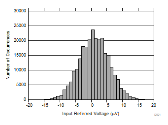
ADS131A02 ADS131A04 D025_sbas590.gif
Shorted inputs, 8 kSPS, 262144 points, offset removed
Figure 10. Single Device Noise Histogram
ADS131A02 ADS131A04 D011_sbas590.gif
fIN = 60 Hz, 32768 points
Figure 12. THD FFT Plot at 8 kSPS and –0.5 dBFS
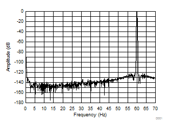
ADS131A02 ADS131A04 D015_sbas590.gif
fIN = 60 Hz, 8 kSPS
Figure 14. Low-Frequency FFT Plot
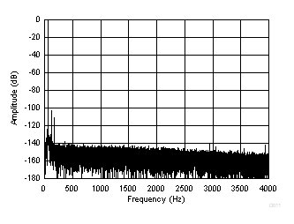
ADS131A02 ADS131A04 D028_sbas590.gif
fIN = 60 Hz, 32768 points
Figure 16. THD FFT Plot at 16 kSPS and –20 dBFS
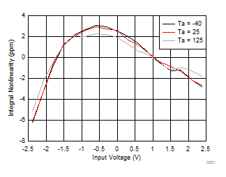
ADS131A02 ADS131A04 D010_sbas590.gif
Figure 18. INL vs Temperature
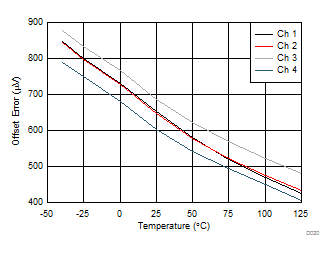
ADS131A02 ADS131A04 D020_sbas590.gif
Figure 20. Offset Error vs Temperature
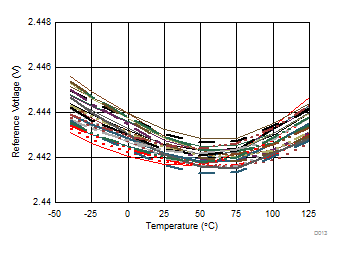
ADS131A02 ADS131A04 D013_sbas590.gif
30 units, multiple lots
Figure 22. Internal VREF vs Temperature
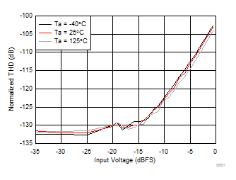
ADS131A02 ADS131A04 D017_sbas590.gif
Figure 24. Normalized THD vs Amplitude
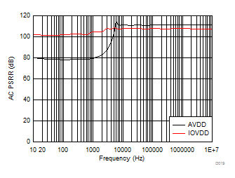
ADS131A02 ADS131A04 D019_sbas590.gif
Figure 26. PSRR vs Frequency
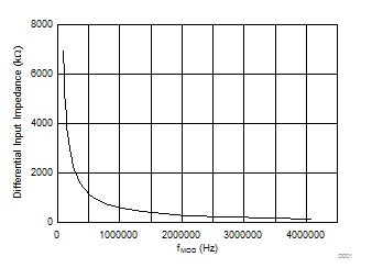
ADS131A02 ADS131A04 D022_sbas590.gif
Figure 28. Differential Input Impedance vs
Modulator Clock
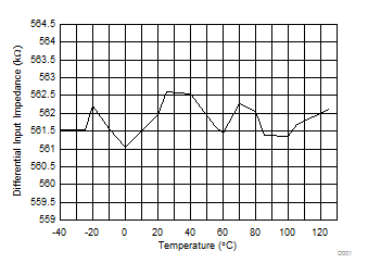
ADS131A02 ADS131A04 D024_sbas590.gif
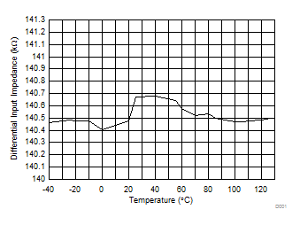
Figure 30. Differential Input Impedance vs
Temperature at 1.024-MHz fMOD
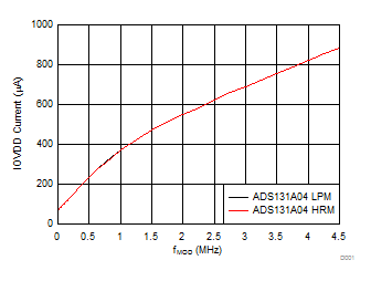
ADS131A02 ADS131A04 D033_sbas590.gif
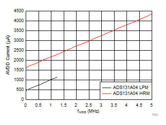
LPM = low-power mode, HRM = high-resolution mode
Figure 32. ADS131A04 IOVDD Current vs fMOD
ADS131A02 ADS131A04 D035_sbas590.gif
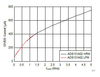
LPM = low-power mode, HRM = high-resolution mode
Figure 34. ADS131A02 IOVDD Current vs fMOD
ADS131A02 ADS131A04 D026_sbas590.gif
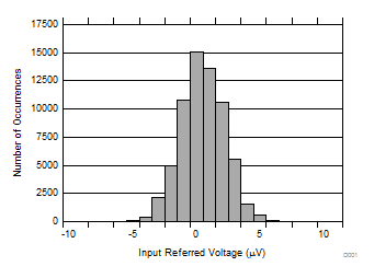
Shorted inputs, 1 kSPS, 65536 points, offset removed
Figure 9. Single Device Noise Histogram
ADS131A02 ADS131A04 D031_sbas590.gif
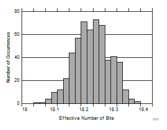
Shorted inputs, 8 kSPS, 560 devices, multiple lots
Figure 11. Multiple Device Effective Resolution Histogram
ADS131A02 ADS131A04 D012_sbas590.gif
fIN = 60 Hz, 32768 points
Figure 13. THD FFT Plot at 8 kSPS and –20 dBFS
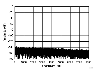
ADS131A02 ADS131A04 D029_sbas590.gif
fIN = 60 Hz, 32768 points
Figure 15. THD FFT Plot at 16 kSPS and –0.5 dBFS
ADS131A02 ADS131A04 D032_sbas590.gif
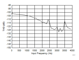
Figure 17. THD vs Input Frequency
ADS131A02 ADS131A04 D018_sbas590.gif
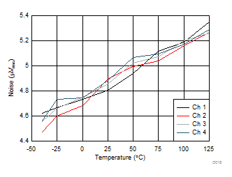
Figure 19. Noise RMS vs Temperature
ADS131A02 ADS131A04 D021_sbas590.gif
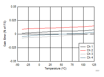
Figure 21. Gain Error vs Temperature
ADS131A02 ADS131A04 D016_sbas590.gif
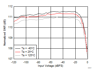
Figure 23. Normalized SNR vs Amplitude
ADS131A02 ADS131A04 D009_sbas590.gif
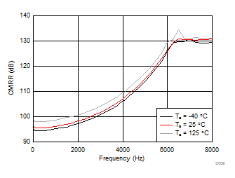
Figure 25. CMRR vs Frequency
ADS131A02 ADS131A04 D030_sbas590.gif
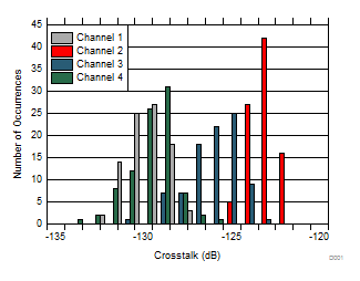
Figure 27. Crosstalk Histogram
ADS131A02 ADS131A04 D023_sbas590.gif
Figure 29. Differential Input Impedance vs
Temperature at 4.096-MHz fMOD
ADS131A02 ADS131A04 D027_sbas590.gif
LPM = low-power mode, HRM = high-resolution mode
Figure 31. ADS131A04 AVDD Current vs fMOD
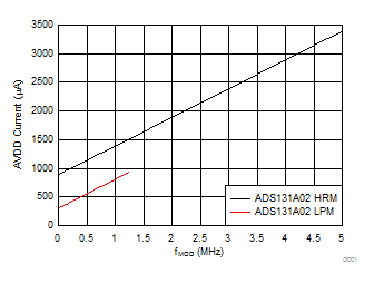
ADS131A02 ADS131A04 D034_sbas590.gif
LPM = low-power mode, HRM = high-resolution mode
Figure 33. ADS131A02 AVDD Current vs fMOD