ZHCSEV8D March 2016 – January 2018 ADS131A02 , ADS131A04
PRODUCTION DATA.
- 1 特性
- 2 应用
- 3 说明
- 4 修订历史记录
- 5 Device Comparison Table
- 6 Pin Configuration and Functions
-
7 Specifications
- 7.1 Absolute Maximum Ratings
- 7.2 ESD Ratings
- 7.3 Recommended Operating Conditions
- 7.4 Thermal Information
- 7.5 Electrical Characteristics
- 7.6 Timing Requirements: Asynchronous Interrupt Interface Mode
- 7.7 Switching Characteristics: Asynchronous Interrupt Interface Mode
- 7.8 Timing Requirements: Synchronous Master Interface Mode
- 7.9 Switching Characteristics: Synchronous Master Interface Mode
- 7.10 Timing Requirements: Synchronous Slave Interface Mode
- 7.11 Switching Characteristics: Synchronous Slave Interface Mode
- 7.12 Typical Characteristics
- 8 Parameter Measurement Information
-
9 Detailed Description
- 9.1 Overview
- 9.2 Functional Block Diagram
- 9.3 Feature Description
- 9.4 Device Functional Modes
- 9.5
Programming
- 9.5.1 Interface Protocol
- 9.5.2 SPI Interface
- 9.5.3
SPI Command Definitions
- 9.5.3.1 NULL: Null Command
- 9.5.3.2 RESET: Reset to POR Values
- 9.5.3.3 STANDBY: Enter Standby Mode
- 9.5.3.4 WAKEUP: Exit STANDBY Mode
- 9.5.3.5 LOCK: Lock ADC Registers
- 9.5.3.6 UNLOCK: Unlock ADC Registers
- 9.5.3.7 RREG: Read a Single Register
- 9.5.3.8 RREGS: Read Multiple Registers
- 9.5.3.9 WREG: Write Single Register
- 9.5.3.10 WREGS: Write Multiple Registers
- 9.6
Register Maps
- 9.6.1
User Register Description
- 9.6.1.1 ID_MSB: ID Control Register MSB (address = 00h) [reset = xxh]
- 9.6.1.2 ID_LSB: ID Control Register LSB (address = 01h) [reset = xxh]
- 9.6.1.3 STAT_1: Status 1 Register (address = 02h) [reset = 00h]
- 9.6.1.4 STAT_P: Positive Input Fault Detect Status Register (address = 03h) [reset = 00h]
- 9.6.1.5 STAT_N: Negative Input Fault Detect Status Register (address = 04h) [reset = 00h]
- 9.6.1.6 STAT_S: SPI Status Register (address = 05h) [reset = 00h]
- 9.6.1.7 ERROR_CNT: Error Count Register (address = 06h) [reset = 00h]
- 9.6.1.8 STAT_M2: Hardware Mode Pin Status Register (address = 07h) [reset = xxh]
- 9.6.1.9 Reserved Registers (address = 08h to 0Ah) [reset = 00h]
- 9.6.1.10 A_SYS_CFG: Analog System Configuration Register (address = 0Bh) [reset = 60h]
- 9.6.1.11 D_SYS_CFG: Digital System Configuration Register (address = 0Ch) [reset = 3Ch]
- 9.6.1.12 CLK1: Clock Configuration 1 Register (address = 0Dh) [reset = 08h]
- 9.6.1.13 CLK2: Clock Configuration 2 Register (address = 0Eh) [reset = 86h]
- 9.6.1.14 ADC_ENA: ADC Channel Enable Register (address = 0Fh) [reset = 00h]
- 9.6.1.15 Reserved Register (address = 10h) [reset = 00h]
- 9.6.2 ADCx: ADC Channel Digital Gain Configuration Registers (address = 11h to 14h) [reset = 00h]
- 9.6.1
User Register Description
- 10Application and Implementation
- 11Power Supply Recommendations
- 12Layout
- 13器件和文档支持
- 14机械、封装和可订购信息
9.3.1 Clock
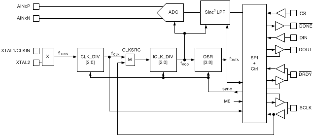
Multiple clocks are created from one external master clock source in the ADS131A0x to create device configuration flexibility. The ADC operates from the internal system clock, ICLK, which is provided in one of three ways.
- An external master clock, CLKIN, can be applied directly to the XTAL1/CLKIN pin to be divided down to generate ICLK using the CLK_DIV[2:0] bits in the CLK1 register. In this case, leave the XTAL2 pin floating.
- A crystal oscillator can be applied between XTAL1/CLKIN and XTAL2, generating a master clock to be divided down using the CLK_DIV[2:0] bits in the CLK1 register to generate ICLK.
- A free-running SCLK can be internally routed to be set as ICLK. This mode is only available in synchronous slave interface mode. Tie the CLKIN/XTAL1 pin to GND. Leave the XTAL2 pin unconnected.
The system ICLK is passed through a second 3-bit clock divider (ICLK_DIV[2:0] in the CLK2 register) to create the modulator clock, MODCLK. MODCLK is used for timing of the delta-sigma (ΔΣ) modulator sampling and digital filter.
The interface operation mode determines the options for sourcing ICLK. When in asynchronous interrupt or synchronous master mode, generate ICLK by applying a direct external master clock signal to the XTAL1/CLKIN pin or by using a crystal oscillator across the XTAL1/CLKIN and XTAL2 pins. If directly applying a master clock to the XTAL1/CLKIN pin, leave XTAL2 floating. In synchronous slave mode, a free-running SCLK line can be connected directly into the ICLK_DIV block in place of the divided XTAL or CLKIN source. Use the CLKSRC bit in the CLK1 register to select between the XTAL1/CLKIN or SCLK input as the master clock source for the ADC. The CLKSRC bit must be set prior to powering up the ADC channels. Using SCLK as ICLK is useful in galvanic isolated applications to limit the digital I/O lines crossing the isolation barrier. Figure 35 shows the clock dividers and clocking names.
 Figure 35. ADC Clock Generation