ZHCSEV8D March 2016 – January 2018 ADS131A02 , ADS131A04
PRODUCTION DATA.
- 1 特性
- 2 应用
- 3 说明
- 4 修订历史记录
- 5 Device Comparison Table
- 6 Pin Configuration and Functions
-
7 Specifications
- 7.1 Absolute Maximum Ratings
- 7.2 ESD Ratings
- 7.3 Recommended Operating Conditions
- 7.4 Thermal Information
- 7.5 Electrical Characteristics
- 7.6 Timing Requirements: Asynchronous Interrupt Interface Mode
- 7.7 Switching Characteristics: Asynchronous Interrupt Interface Mode
- 7.8 Timing Requirements: Synchronous Master Interface Mode
- 7.9 Switching Characteristics: Synchronous Master Interface Mode
- 7.10 Timing Requirements: Synchronous Slave Interface Mode
- 7.11 Switching Characteristics: Synchronous Slave Interface Mode
- 7.12 Typical Characteristics
- 8 Parameter Measurement Information
-
9 Detailed Description
- 9.1 Overview
- 9.2 Functional Block Diagram
- 9.3 Feature Description
- 9.4 Device Functional Modes
- 9.5
Programming
- 9.5.1 Interface Protocol
- 9.5.2 SPI Interface
- 9.5.3
SPI Command Definitions
- 9.5.3.1 NULL: Null Command
- 9.5.3.2 RESET: Reset to POR Values
- 9.5.3.3 STANDBY: Enter Standby Mode
- 9.5.3.4 WAKEUP: Exit STANDBY Mode
- 9.5.3.5 LOCK: Lock ADC Registers
- 9.5.3.6 UNLOCK: Unlock ADC Registers
- 9.5.3.7 RREG: Read a Single Register
- 9.5.3.8 RREGS: Read Multiple Registers
- 9.5.3.9 WREG: Write Single Register
- 9.5.3.10 WREGS: Write Multiple Registers
- 9.6
Register Maps
- 9.6.1
User Register Description
- 9.6.1.1 ID_MSB: ID Control Register MSB (address = 00h) [reset = xxh]
- 9.6.1.2 ID_LSB: ID Control Register LSB (address = 01h) [reset = xxh]
- 9.6.1.3 STAT_1: Status 1 Register (address = 02h) [reset = 00h]
- 9.6.1.4 STAT_P: Positive Input Fault Detect Status Register (address = 03h) [reset = 00h]
- 9.6.1.5 STAT_N: Negative Input Fault Detect Status Register (address = 04h) [reset = 00h]
- 9.6.1.6 STAT_S: SPI Status Register (address = 05h) [reset = 00h]
- 9.6.1.7 ERROR_CNT: Error Count Register (address = 06h) [reset = 00h]
- 9.6.1.8 STAT_M2: Hardware Mode Pin Status Register (address = 07h) [reset = xxh]
- 9.6.1.9 Reserved Registers (address = 08h to 0Ah) [reset = 00h]
- 9.6.1.10 A_SYS_CFG: Analog System Configuration Register (address = 0Bh) [reset = 60h]
- 9.6.1.11 D_SYS_CFG: Digital System Configuration Register (address = 0Ch) [reset = 3Ch]
- 9.6.1.12 CLK1: Clock Configuration 1 Register (address = 0Dh) [reset = 08h]
- 9.6.1.13 CLK2: Clock Configuration 2 Register (address = 0Eh) [reset = 86h]
- 9.6.1.14 ADC_ENA: ADC Channel Enable Register (address = 0Fh) [reset = 00h]
- 9.6.1.15 Reserved Register (address = 10h) [reset = 00h]
- 9.6.2 ADCx: ADC Channel Digital Gain Configuration Registers (address = 11h to 14h) [reset = 00h]
- 9.6.1
User Register Description
- 10Application and Implementation
- 11Power Supply Recommendations
- 12Layout
- 13器件和文档支持
- 14机械、封装和可订购信息
10.3 Do's and Don'ts
- Do partition the analog, digital, and power-supply circuitry into separate sections on the printed circuit board (PCB).
- Do use a single ground plane for analog and digital grounds.
- Do place the analog components close to the ADC pins using short, direct connections.
- Do keep the SCLK pin free of glitches and noise.
- Do verify that the analog input voltages are within the specified voltage range under all input conditions.
- Do tie unused analog input pins to GND.
- Do provide current limiting to the analog inputs in case overvoltage faults occur.
- Do use a low-dropout (LDO) regulator to reduce ripple voltage generated by switch-mode power supplies. This reduction is especially true for AVDD where the supply noise can affect performance.
- Do keep the input series resistance low to maximize THD performance.
- Do not cross analog and digital signals.
- Do not allow the analog power supply voltages (AVDD – AVSS) to exceed 3.6 V under any conditions, including during power-up and power-down when the negative charge pump is enabled.
- Do not allow the analog power supply voltages (AVDD – AVSS) to exceed 6 V under any conditions, including during power-up and power-down when the negative charge pump is disabled.
- Do not allow the digital supply voltage to exceed 3.9 V under any conditions, including during power-up and power-down.
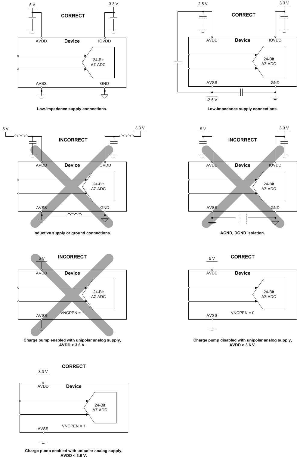
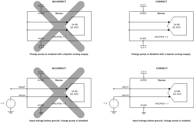
Figure 104 and Figure 105 illustrate correct and incorrect ADC circuit connections.
 Figure 104. Correct and Incorrect Circuit Connections
 Figure 105. Correct and Incorrect Circuit Connections, Continued