ZHCSN81 july   2023 ADS131B23-Q1

PRODUCTION DATA  

  1.   1
  2. 特性
  3. 应用
  4. 说明
  5. Revision History
  6. 说明(续)
  7. Pin Configuration and Functions
  8. Specifications
    1. 7.1 Absolute Maximum Ratings
    2. 7.2 ESD Ratings
    3. 7.3 Recommended Operating Conditions
    4. 7.4 Thermal Information
    5. 7.5 Electrical Characteristics
    6. 7.6 Timing Requirements
    7. 7.7 Switching Characteristics
    8. 7.8 Timing Diagram
    9. 7.9 Typical Characteristics
  9. Parameter Measurement Information
    1. 8.1 Offset Drift Measurement
    2. 8.2 Gain Drift Measurement
    3. 8.3 Noise Performance
  10. Detailed Description
    1. 9.1 Overview
    2. 9.2 Functional Block Diagram
    3. 9.3 Feature Description
      1. 9.3.1 Naming Conventions
      2. 9.3.2 Precision Voltage References (REFA, REFB)
      3. 9.3.3 Clocking (MCLK, OSCM, OSCD)
      4. 9.3.4 ADC1y
        1. 9.3.4.1 ADC1y Input Multiplexer
        2. 9.3.4.2 ADC1y Programmable Gain Amplifier (PGA)
        3. 9.3.4.3 ADC1y ΔΣ Modulator
        4. 9.3.4.4 ADC1y Digital Filter
        5. 9.3.4.5 ADC1y Offset and Gain Calibration
        6. 9.3.4.6 ADC1y Conversion Data
      5. 9.3.5 ADC2y
        1. 9.3.5.1 ADC2y Input Multiplexer
        2. 9.3.5.2 ADC2y Programmable Gain Amplifier (PGA)
        3. 9.3.5.3 ADC2y ΔΣ Modulator
        4. 9.3.5.4 ADC2y Digital Filter
        5. 9.3.5.5 ADC2y Offset and Gain Calibration
        6. 9.3.5.6 ADC2y Sequencer
        7. 9.3.5.7 VCMy Buffers
        8. 9.3.5.8 ADC2y Measurement Configurations
        9. 9.3.5.9 ADC2y Conversion Data
      6. 9.3.6 General-Purpose Digital Inputs and Outputs (GPIO0 to GPIO4)
        1. 9.3.6.1 GPIOx PWM Output Configuration
        2. 9.3.6.2 GPIOx PWM Input Readback
      7. 9.3.7 General-Purpose Digital Inputs and Outputs (GPIO0A, GPIO1A, GPIO0B, GPIO1B)
      8. 9.3.8 Monitors and Diagnostics
        1. 9.3.8.1  Supply Monitors
        2. 9.3.8.2  Clock Monitors
        3. 9.3.8.3  Digital Monitors
          1. 9.3.8.3.1 Register Map CRC
          2. 9.3.8.3.2 Memory Map CRC
          3. 9.3.8.3.3 GPIO Readback
        4. 9.3.8.4  Communication Monitors
        5. 9.3.8.5  Fault Flags and Fault Masking
        6. 9.3.8.6  FAULT Pin
        7. 9.3.8.7  Diagnostics and Diagnostic Procedure
        8. 9.3.8.8  Indicators
        9. 9.3.8.9  Conversion and Sequence Counters
        10. 9.3.8.10 Supply Voltage Readback
        11. 9.3.8.11 Temperature Sensor (TSA)
        12. 9.3.8.12 Test DACs (TDACA, TDACB)
        13. 9.3.8.13 Open-Wire Detection
        14. 9.3.8.14 Missing Host Detection and MHD Pin
        15. 9.3.8.15 Overcurrent Comparators (OCCA, OCCB)
          1. 9.3.8.15.1 OCCA and OCCB Pins
          2. 9.3.8.15.2 Overcurrent Indication Response Time
    4. 9.4 Device Functional Modes
      1. 9.4.1 Power-Up and Reset
        1. 9.4.1.1 Power-On Reset (POR)
        2. 9.4.1.2 RESETn Pin
        3. 9.4.1.3 RESET Command
      2. 9.4.2 Operating Modes
        1. 9.4.2.1 Active Mode
        2. 9.4.2.2 Standby Mode
        3. 9.4.2.3 Power-Down Mode
      3. 9.4.3 ADC Conversion Modes
        1. 9.4.3.1 ADC1y Conversion Modes
          1. 9.4.3.1.1 Continuous-Conversion Mode
          2. 9.4.3.1.2 Single-Shot Conversion Mode
          3. 9.4.3.1.3 Global-Chop Mode
            1. 9.4.3.1.3.1 Overcurrent Indication Response Time in Global-Chop Mode
        2. 9.4.3.2 ADC2y Sequencer Operation and Sequence Modes
          1. 9.4.3.2.1 Continuous Sequence Mode
          2. 9.4.3.2.2 Single-Shot Sequence Mode
          3. 9.4.3.2.3 Synchronized Single-Shot Sequence Mode Based on ADC1y Conversion Starts
    5. 9.5 Programming
      1. 9.5.1 Serial Interface
        1. 9.5.1.1 Serial Interface Signals
          1. 9.5.1.1.1 Chip Select (CSn)
          2. 9.5.1.1.2 Serial Data Clock (SCLK)
          3. 9.5.1.1.3 Serial Data Input (SDI)
          4. 9.5.1.1.4 Serial Data Output (SDO)
          5. 9.5.1.1.5 Data Ready (DRDYn)
        2. 9.5.1.2 Serial Interface Communication Structure
          1. 9.5.1.2.1 SPI Communication Frames
          2. 9.5.1.2.2 SPI Communication Words
          3. 9.5.1.2.3 STATUS Word
          4. 9.5.1.2.4 Communication Cyclic Redundancy Check (CRC)
          5. 9.5.1.2.5 Commands
            1. 9.5.1.2.5.1 NULL (0000 0000 0000 0000b)
            2. 9.5.1.2.5.2 RESET (0000 0000 0001 0001b)
            3. 9.5.1.2.5.3 LOCK (0000 0101 0101 0101b)
            4. 9.5.1.2.5.4 UNLOCK (0000 0110 0101 0101b)
            5. 9.5.1.2.5.5 WREG (011a aaaa aaa0 0nnnb)
            6. 9.5.1.2.5.6 RREG (101a aaaa aaan nnnnb)
          6. 9.5.1.2.6 SCLK Counter
          7. 9.5.1.2.7 SPI Timeout
          8. 9.5.1.2.8 Reading ADC1A, ADC1B, and ADC2A Conversion Data
          9. 9.5.1.2.9 DRDYn Pin Behavior
    6. 9.6 Register Map
      1. 9.6.1 Registers
  11. 10Application and Implementation
    1. 10.1 Application Information
      1. 10.1.1 Unused Inputs and Outputs
      2. 10.1.2 Minimum Interface Connections
    2. 10.2 Typical Application
      1. 10.2.1 Design Requirements
      2. 10.2.2 Detailed Design Procedure
        1. 10.2.2.1 Current Shunt Measurement
        2. 10.2.2.2 Battery Pack Voltage Measurement
        3. 10.2.2.3 Shunt Temperature Measurement
      3. 10.2.3 Application Curves
    3. 10.3 Power Supply Recommendations
      1. 10.3.1 Power-Supply Options
        1. 10.3.1.1 Single Unregulated External 4-V to 16-V Supply (3.3-V Digital I/O Levels)
        2. 10.3.1.2 Single Regulated External 3.3-V Supply (3.3-V Digital IO Levels)
        3. 10.3.1.3 Single Regulated External 5-V Supply (5-V Digital I/O Levels)
      2. 10.3.2 Power-Supply Sequencing
      3. 10.3.3 Power-Supply Decoupling
    4. 10.4 Layout
      1. 10.4.1 Layout Guidelines
      2. 10.4.2 Layout Example
  12. 11Device and Documentation Support
    1. 11.1 Documentation Support
      1. 11.1.1 Related Documentation
    2. 11.2 接收文档更新通知
    3. 11.3 支持资源
    4. 11.4 Trademarks
    5. 11.5 静电放电警告
    6. 11.6 术语表
  13. 12Mechanical, Packaging, and Orderable Information

封装选项

机械数据 (封装 | 引脚)
散热焊盘机械数据 (封装 | 引脚)
订购信息

ADC1y Conversion Data

Conversion data for ADC1A and ADC1B are 24 bits and are automatically output on SDO as part of the SPI frame, unless register data are output following a register read command.

Data are provided in binary two's-complement format. Use Equation 8 to calculate the size of one code (LSB).

Equation 8. 1 LSB = (2 × VREFy / Gain) / 224 = +FSR / 223

A positive full-scale input VIN ≥ +FSR – 1 LSB = VREFy / Gain – 1 LSB produces an output code of 7FFFFFh and a negative full-scale input (VIN ≤ –FSR = –VREFy / Gain) produces an output code of 800000h. The output clips at these codes for signals that exceed full-scale.

Table 9-7 summarizes the ideal output codes for different input signals.

Table 9-7 Ideal Output Code versus Input Signal (24-Bit Conversion Data)
INPUT SIGNAL
(VIN = VAINP – VAINN)
IDEAL OUTPUT CODE
≥ FSR (223 – 1) / 223 7FFFFFh
FSR / 223 000001h
0 000000h
–FSR / 223 FFFFFFh
≤ –FSR 800000h

Figure 9-6 shows the mapping of the analog input signal to the output codes.
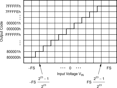
GUID-63066F35-94D2-4816-AF23-A32C628FD3B1-low.gif Figure 9-6 Code Transition Diagram (24-Bit Conversion Data)