ZHCS960C June 2012 – January 2017 ADS131E04 , ADS131E06 , ADS131E08
PRODUCTION DATA.
- 1 特性
- 2 应用
- 3 说明
- 4 修订历史记录
- 5 Device Comparison
- 6 Pin Configuration and Functions
- 7 Specifications
- 8 Parameter Measurement Information
-
9 Detailed Description
- 9.1 Overview
- 9.2 Functional Block Diagram
- 9.3 Feature Description
- 9.4 Device Functional Modes
- 9.5
Programming
- 9.5.1 Data Format
- 9.5.2 SPI Interface
- 9.5.3
SPI Command Definitions
- 9.5.3.1 Sending Multibyte Commands
- 9.5.3.2 WAKEUP: Exit STANDBY Mode
- 9.5.3.3 STANDBY: Enter STANDBY Mode
- 9.5.3.4 RESET: Reset Registers to Default Values
- 9.5.3.5 START: Start Conversions
- 9.5.3.6 STOP: Stop Conversions
- 9.5.3.7 OFFSETCAL: Channel Offset Calibration
- 9.5.3.8 RDATAC: Start Read Data Continuous Mode
- 9.5.3.9 SDATAC: Stop Read Data Continuous Mode
- 9.5.3.10 RDATA: Read Data
- 9.5.3.11 RREG: Read from Register
- 9.5.3.12 WREG: Write to Register
- 9.6
Register Map
- 9.6.1
Register Descriptions
- 9.6.1.1 ID: ID Control Register (Factory-Programmed, Read-Only) (address = 00h) [reset = xxh]
- 9.6.1.2 CONFIG1: Configuration Register 1 (address = 01h) [reset = 91h]
- 9.6.1.3 CONFIG2: Configuration Register 2 (address = 02h) [reset = E0h]
- 9.6.1.4 CONFIG3: Configuration Register 3 (address = 03h) [reset = 40]
- 9.6.1.5 FAULT: Fault Detect Control Register (address = 04h) [reset = 00h]
- 9.6.1.6 CHnSET: Individual Channel Settings (address = 05h to 0Ch) [reset = 10h]
- 9.6.1.7 FAULT_STATP: Fault Detect Positive Input Status (address = 12h) [reset = 00h]
- 9.6.1.8 FAULT_STATN: Fault Detect Negative Input Status (address = 13h) [reset = 00h]
- 9.6.1.9 GPIO: General-Purpose IO Register (address = 14h) [reset = 0Fh]
- 9.6.1
Register Descriptions
- 10Application and Implementation
- 11Power Supply Recommendations
- 12Layout
- 13器件和文档支持
- 14机械、封装和可订购信息
9 Detailed Description
9.1 Overview
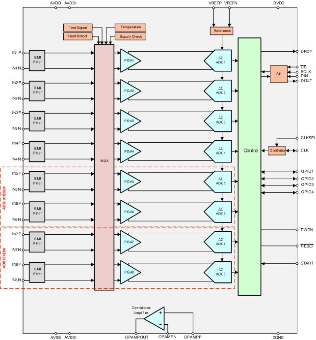
The ADS131E0x series are low-power, multichannel, simultaneously-sampling, 24-bit, delta-sigma (ΔΣ), analog-to-digital converter (ADC) with an integrated programmable gain amplifier (PGA). The analog device performance across a scalable data rate makes the device well-suited for smart-grid and other industrial power monitor, control, and protection applications.
The ADS131E0x devices have a programmable multiplexer that allows for various internal monitoring signal measurements including temperature, supply, and input-short for device noise testing. The PGA gain can be chosen from one of five settings: 1, 2, 4, 8, or 12. The ADCs in the device offer data rates of 1 kSPS, 2 kSPS, 4 kSPS, 8 kSPS, 16 kSPS, 32 kSPS, and 64 kSPS. The devices communicate using a serial peripheral interface (SPI)-compatible interface. The devices provide four general-purpose I/O (GPIO) pins for general use. Use multiple devices to easily add channels to the system and synchronize them with the START pins.
Program the internal reference to either 2.4 V or 4 V. The internal oscillator generates a 2.048-MHz clock. Use the integrated comparators, with programmable trigger-points, for input overrange or underrange detection. A detailed diagram of the ADS131E0x is provided in .
9.2 Functional Block Diagram
9.3 Feature Description
9.3.1 Electromagnetic Interference (EMI) Filter
An RC filter at the input functions as an EMI filter on all channels. The –3-dB filter bandwidth is approximately 3 MHz.
9.3.2 Input Multiplexer
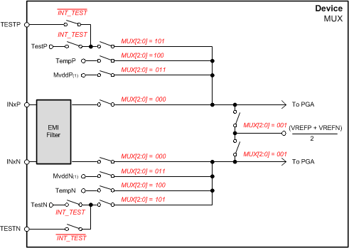
The ADS131E0x input multiplexers are very flexible and provide many configurable signal-switching options. Figure 16 shows a diagram of the multiplexer on a single channel of the device. INxP and INxN are separate for each of the four, six or eight blocks (depending on device). This flexibility allows for significant device and sub-system diagnostics, calibration, and configuration. Switch settings for each channel are selected by writing the appropriate values to the CHnSET registers (see the CHnSET registers in the Register Map section for details). The output of each multiplexer is connected to the individual channel PGA.
9.3.2.1 Device Noise Measurements
Setting CHnSET[2:0] = 001 sets the common-mode voltage of [(VVREFP + VVREFN) / 2] to both channel inputs. Use this setting to test inherent device noise in the user system.
9.3.2.2 Test Signals (TestP and TestN)
Setting CHnSET[2:0] = 101 provides internally-generated test signals for use in sub-system verification at power-up. The test signals are controlled through register settings (see the CONFIG2: Configuration Register 2 section for details). TEST_AMP controls the signal amplitude and TEST_FREQ controls the switching frequency of the test signal. The test signals are multiplexed and transmitted out of the device at the TESTP and TESTN pins. The INT_TEST register bit (in the CONFIG2: Configuration Register 2 section) deactivates the internal test signals so that the test signal can be driven externally. This feature allows the test or calibration of multiple devices with the same signal.
9.3.2.3 Temperature Sensor (TempP, TempN)
Setting CHnSET[2:0] = 100 sets the channel input to the temperature sensor. This sensor uses two internal diodes with one diode having a current density 16 times that of the other, as shown in Figure 17. The difference in diode current densities yields a difference in voltage that is proportional to absolute temperature.
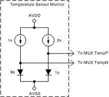 Figure 17. Temperature Sensor Implementation
The internal device temperature tracks the PCB temperature closely because of the low thermal resistance of the package to the PCB. Self-heating of the ADS131E0x causes a higher reading than the temperature of the surrounding PCB. Setting the channel gain to 1 is recommended when the temperature measurement is taken.
The scale factor of Equation 3 converts the temperature reading to °C. Before using this equation, the temperature reading code must first be scaled to μV.

9.3.2.4 Power-Supply Measurements (MVDDP, MVDDN)
Setting CHnSET[2:0] = 011 sets the channel inputs to different device supply voltages. For channels 1, 2, 5, 6, 7, and 8 (MVDDP – MVDDN) is [0.5 × (AVDD – AVSS)]; for channels 3 and 4 (MVDDP – MVDDN) is
DVDD / 4. Set the gain to 1 to avoid saturating the PGA when measuring power supplies.
9.3.3 Analog Input
The analog inputs to the device connect directly to an integrated low-noise, low-drift, high input impedance, programmable gain amplifier. The amplifier is located following the individual channel multiplexer.
The ADS131E0x analog inputs are fully differential. The differential input voltage (VINxP – VINxN) can span from –VREF / gain to VREF / gain. See the Data Format section for an explanation of the correlation between the analog input and digital codes. There are two general methods of driving the ADS131E0x analog inputs: pseudo-differential or fully-differential, as shown in Figure 18, Figure 19, and Figure 20.
 Figure 18. Methods of Driving the ADS131E0x: Pseudo-Differential or Fully Differential
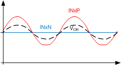 Figure 19. Pseudo-Differential Input Mode
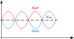 Figure 20. Fully-Differential Input Mode
Hold the INxN pin at a common voltage, preferably at mid supply, to configure the fully differential input for a pseudo-differential signal. Swing the INxP pin around the common voltage –VREF / gain to VREF / gain and remain within the absolute maximum specifications. Verify that the differential signal at the minimum and maximum points meets the common-mode input specification discussed in the Input Common-Mode Range section.
Configure the signals at INxP and INxN to be 180° out-of-phase centered around a common-mode voltage, VCM, to use a fully-differential input method. Both the INxP and INxN inputs swing from the VCM + ½ VREF / gain to the VCM – ½ VREF / gain. The differential voltage at the maximum and minimum points is equal to –VREF / gain to VREF / gain. Use the ADS131E0x in a differential configuration to maximize the dynamic range of the data converter. For optimal performance, the common-mode voltage is recommended to be set at the midpoint of the analog supplies [(AVDD + AVSS) / 2].
If any of the analog input channels are not used, then power-down these pins using register bits to conserve power. See the SPI Command Definitions section for more information on how to power-down individual channels. Tie any unused or powered down analog input pins directly to AVDD.
9.3.4 PGA Settings and Input Range
Each channel has its own configurable programmable gain amplifier (PGA) following its multiplexer. The PGA is designed using two operational amplifiers in a differential configuration, as shown in Figure 21. Set the gain to one of five settings (1, 2, 4, 8, and 12) using the CHnSET registers for each individual channel (see the CHnSET registers in the Register Map section for details). The ADS131E0x has CMOS inputs and therefore has negligible current noise. Table 3 shows the typical small-signal bandwidth values for various gain settings.
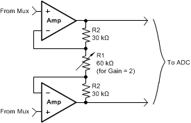 Figure 21. PGA Implementation
Table 3. PGA Gain versus Bandwidth
| GAIN | NOMINAL BANDWIDTH AT TA = 25°C (kHz) |
|---|---|
| 1 | 237 |
| 2 | 146 |
| 4 | 96 |
| 8 | 48 |
| 12 | 32 |
The PGA resistor string that implements the gain has 120 kΩ of resistance for a gain of 2. This resistance provides a current path across the PGA outputs in the presence of a differential input signal. This current is in addition to the quiescent current specified for the device in the presence of a differential signal at the input.
9.3.4.1 Input Common-Mode Range
The usable input common-mode range of the analog front-end depends on various parameters, including the maximum differential input signal, supply voltage, and PGA gain. The common-mode range, VCM, is defined in Equation 4:

where
- VMAX_DIFF = maximum differential signal at the PGA input and
- VCM = common-mode voltage
For example:
If AVDD – AVSS = 3.3 V, gain = 2, and VMAX_DIFF = 1000 mV,
Then 1.3 V < VCM < 2.0 V
9.3.5 ΔΣ Modulator
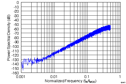
Each ADS131E0x channel has its own delta-sigma (ΔΣ) ADC. The ΔΣ converters use second-order modulators optimized for low-power applications. The modulator samples the input signal at the modulator rate of (fMOD = fCLK / 2). As with any ΔΣ modulator, the ADS131E0x noise is shaped until fMOD / 2, as shown in Figure 22.
9.3.6 Clock
The ADS131E0x provides two different device clocking methods: internal and external. Internal clocking using the internal oscillator is ideally-suited for non-synchronized, low-power systems. The internal oscillator is trimmed for accuracy at room temperature. The accuracy of the internal oscillator varies over the specified temperature range; see the Electrical Characteristics table for details. External clocking is recommended when synchronizing multiple ADS131E0x devices or when synchronizing to an external event because the internal oscillator clock performance can vary over temperature. Clock selection is controlled by the CLKSEL pin and the CLK_EN register bit. Provide the external clock any time after the analog and digital supplies are present.
The CLKSEL pin selects either the internal oscillator or external clock. The CLK_EN bit in the CONFIG1 register enables and disables the oscillator clock to be output on the CLK pin. A truth table for the CLKSEL pin and the CLK_EN bit is shown in Table 4. The CLK_EN bit is useful when multiple devices are used in a daisy-chain configuration. During power-down, the external clock is recommended to be shut down to save power.
Table 4. CLKSEL Pin and CLK_EN Bit
| CLKSEL PIN | CLK_EN BIT | CLOCK SOURCE | CLK PIN STATUS |
|---|---|---|---|
| 0 | X | External clock | Input: external clock |
| 1 | 0 | Internal oscillator | 3-state |
| 1 | 1 | Internal oscillator | Output: internal oscillator |
9.3.7 Digital Decimation Filter
The digital filter receives the modulator output bit stream and decimates the data stream. The decimation ratio determines the number of samples taken to create the output data word, and is set by the modulator rate divided by the data rate (fMOD / fDR). By adjusting the decimation ratio, a tradeoff can be made between resolution and data rate: higher decimation allows for higher resolution (thus creating lower data rates) and lower decimation decreases resolution but enables wider bandwidths with higher data rates. Higher data rates are typically used in power applications that implement software re-sampling techniques to help with channel-to-channel phase adjustment for voltage and current.
The digital filter on each channel consists of a third-order sinc filter. An input step change takes three conversion cycles for the filter to settle. Adjust the decimation ratio of the sinc3 filters using the DR[2:0] bits in the CONFIG1 register (see the Register Map section for details). The data rate setting is a global setting that sets all channels to the same data rate.
The sinc filter is a variable decimation rate, third-order, low-pass filter. Data are supplied to this section of the filter from the modulator at the rate of fMOD. The sinc3 filter attenuates the high-frequency modulator noise, then decimates the data stream into parallel data. The decimation rate affects the overall converter data rate.
Equation 5 shows the scaled sinc3 filter Z-domain transfer function.

The sinc3 filter frequency domain transfer function is shown in Equation 6.
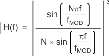
where
- N = decimation ratio
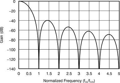
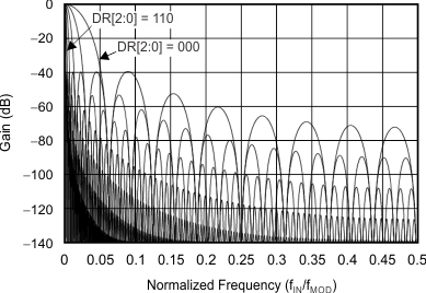
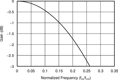
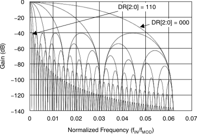
The sinc3 filter has notches (or zeroes) that occur at the output data rate and multiples thereof. At these frequencies, the filter has infinite attenuation. Figure 23 illustrates the sinc filter frequency response and Figure 24 illustrates the sinc filter roll-off. Figure 25 and Figure 26 illustrate the filter transfer function until fMOD / 2 and fMOD / 16, respectively, at different data rates. Figure 27 illustrates the transfer function extended until 4 fMOD. Figure 27 illustrates that the ADS131E0x passband repeats itself at every fMOD. Note that the digital filter response and filter notches are proportional to the master clock frequency.
![ADS131E04 ADS131E06 ADS131E08 Transfer Function
of Decimation Filters
Until 4 fMOD for DR[2:0] = 000 and DR[2:0] = 110 ADS131E04 ADS131E06 ADS131E08 ai_tx_funct_bas561.gif](/ods/images/ZHCS960C/ai_tx_funct_bas561.gif)
Until 4 fMOD for DR[2:0] = 000 and DR[2:0] = 110
9.3.8 Voltage Reference
Figure 28 shows a simplified block diagram of the internal ADS131E0x reference. The reference voltage is generated with respect to AVSS. When using the internal voltage reference, connect VREFN to AVSS.
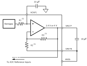
The external band-limiting capacitors determine the amount of reference noise contribution. For high-end systems, the capacitor values should be chosen such that the bandwidth is limited to less than 10 Hz, so that the reference noise does not dominate the system noise. When using a 3-V analog supply, the internal reference must be set to 2.4 V. In case of a 5-V analog supply, the internal reference can be set to 4 V by setting the VREF_4V bit in the CONFIG2 register.
Alternatively, the internal reference buffer can be powered down and VREFP can be driven externally. Figure 29 shows a typical external reference drive circuit. Power-down is controlled by the PD_REFBUF bit in the CONFIG3 register. This power-down is also used to share internal references when two devices are cascaded. By default, the device wakes up in external reference mode.
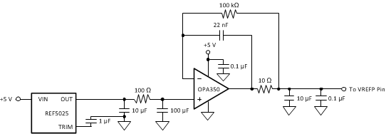 Figure 29. External Reference Driver
9.3.9 Input Out-of-Range Detection
The ADS131E0x has integrated comparators to detect out-of-range conditions on the input signals. The basic principle is to compare the input voltage against a threshold voltage set by a 3-bit digital-to-analog converter (DAC) based off the analog power supply. The comparator trigger threshold level is set by the COMP_TH[2:0] bits in the FAULT register.
If the ADS131E0x is powered from a ±2.5-V supply and COMP_TH[2:0] = 000 (95% and 5%), the high-side trigger threshold is set at 2.25 V [equal to AVSS + (AVDD – AVSS) × 95%] and the low-side threshold is set at –2.25 V [equal to AVSS + (AVDD – AVSS) × 5%]. The threshold calculation formula applies to unipolar as well as to bipolar supplies.
A fault condition can be detected by setting the appropriate threshold level using the COMP_TH[2:0] bits. To determine which of the inputs is out of range, read the FAULT_STATP and FAULT_STATN registers individually or read the FAULT_STATx bits as part of the output data stream; see the Data Output (DOUT) section.
9.3.10 General-Purpose Digital I/O (GPIO)
The ADS131E0x has a total of four general-purpose digital I/O (GPIO) pins available. Configure the digital I/O pins as either inputs or outputs through the GPIOC bits. The GPIOD bits in the GPIO register indicate the level of the pins. The GPIO logic high voltage level is set by the voltage level of DVDD. When reading the GPIOD bits, the data returned are the logic level of the pins, whether they are programmed as inputs or outputs. When the GPIO pin is configured as an input, a write to the corresponding GPIOD bit has no effect. When configured as an output, a write to the GPIOD bit sets the output level.
If configured as inputs, the GPIO pins must be driven to a defined state. The GPIO pins are set as inputs after power up or after a reset. Figure 30 shows the GPIO pin structure. Connect unused GPIO pins directly to DGND through 10-kΩ resistors.
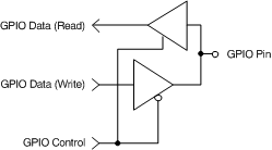 Figure 30. GPIO Pin Implementation
9.4 Device Functional Modes
9.4.1 Start
Pull the START pin high for at least 2 tCLK periods, or send the START command to begin conversions. When START is low and the START command has not been sent, the device does not issue a DRDY signal (conversions are halted).
When using the START command to control conversions, hold the START pin low. In multiple device configurations, the START pin is used to synchronize devices (see the Multiple Device Configuration subsection for more details).
9.4.1.1 Settling Time
The settling time (tSETTLE) is the time required for the converter to output fully-settled data when the START signal is pulled high. When START is pulled high, DRDY is also pulled high. The next DRDY falling edge indicates that data are ready. Figure 31 shows the timing diagram and Table 5 shows the settling time for different data rates as a function of tCLK. The settling time depends on fCLK and the decimation ratio (controlled by the DR[2:0] bits in the CONFIG1 register). When the initial settling time has passed, the DRDY falling edge occurs at the set data rate, tDR. If data is not read back on DOUT and the output shift register needs to update, DRDY goes high for 4 tCLK before returning back low indicating new data is ready. Note that when START is held high and there is a step change in the input signal, 3 × tDR is required for the filter to settle to the new value. Settled data are available on the fourth DRDY pulse.
Table 5. Settling Time for Different Data Rates
| DR[2:0] | NORMAL MODE | UNIT |
|---|---|---|
| 000 | 152 | tCLK |
| 001 | 296 | tCLK |
| 010 | 584 | tCLK |
| 011 | 1160 | tCLK |
| 100 | 2312 | tCLK |
| 101 | 4616 | tCLK |
| 110 | 9224 | tCLK |
9.4.1.2 Input Signal Step
When the device is converting and there is a step change on the input signal, a delay of 3 tDR is required for the output data to settle. Settled data are available on the fourth DRDY pulse. Data are available to read at each DRDY low transition prior to the 4th DRDY pulse, but are recommended to be ignored. Figure 32 shows the required wait time for complete settling for an input step or input transient event on the analog input.
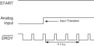 Figure 32. Settling Time for the Input Transient
9.4.2 Reset (RESET)
There are two methods to reset the ADS131E0x: pull the RESET pin low, or send the RESET command. When using the RESET pin, make sure to follow the minimum pulse duration timing specifications before taking the pin back high. The RESET command takes effect on the eighth SCLK falling edge of the command. After a reset, 18 tCLK cycles are required to complete initialization of the configuration registers to default states and start the conversion cycle. Note that an internal reset is automatically issued to the digital filter whenever the CONFIG1 register is set to a new value with a WREG command.
9.4.3 Power-Down (PWDN)
When PWDN is pulled low, all on-chip circuitry is powered down. To exit power-down mode, take the PWDN pin high. Upon exiting from power-down mode, the internal oscillator and the reference require time to wake up. During power-down, the external clock is recommended to be shut down to save power.
9.4.4 Continuous Conversion Mode
Conversions begin when the START pin is taken high or when the START command is sent. As shown in Figure 33, the DRDY output goes high when conversions are started and goes low when data are ready. Conversions continue indefinitely until the START pin is taken low or the STOP command is transmitted. When the START pin is pulled low or the STOP command is issued, the conversion in progress is allowed to complete. Figure 34 and Table 6 show the required DRDY timing to the START pin or the START and STOP commands when controlling conversions in this mode. The tSDSU timing indicates when to take the START pin low or when to send the STOP command before the DRDY falling edge to halt further conversions. The tDSHD timing indicates when to take the START pin low or send the STOP command after a DRDY falling edge to complete the current conversion and halt further conversions. To keep the converter running continuously, the START pin can be permanently tied high.
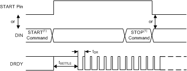

Table 6. Timing Characteristics for Figure 34(1)
| MIN | UNIT | ||
|---|---|---|---|
| tSDSU | Setup time: START pin low or STOP command before the DRDY falling edge to halt further conversions | 16 | tCLK |
| tDSHD | Delay time: START pin low or STOP command to complete the current conversion and halt further conversions | 16 | tCLK |
9.4.5 Data Retrieval
9.4.5.1 Data Ready (DRDY)
DRDY is an output signal which transitions from high to low indicating new conversion data are ready. The CS signal has no effect on the data ready signal. DRDY behavior is determined by whether the device is in RDATAC mode or the RDATA command is used to read data on demand. (See the RDATAC: Start Read Data Continuous Mode and RDATA: Read Data subsections of the SPI Command Definitions section for further details).
When reading data with the RDATA command, the read operation can overlap the next DRDY occurrence without data corruption.
The START pin or the START command places the device either in normal data capture mode or pulse data capture mode.
Figure 35 shows the relationship between CS, DRDY, DOUT, and SCLK during data retrieval (in case of an ADS131E0x). DOUT is latched out at the SCLK rising edge. DRDY is pulled high at the SCLK falling edge. Note that DRDY goes high on the first SCLK falling edge, regardless of whether data are being retrieved from the device or a command is being sent through the DIN pin.
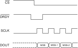 Figure 35. DRDY Behavior with Data Retrieval
The DRDY signal is cleared on the first SCLK falling edge regardless of the state of CS. This condition must be taken into consideration if the SPI bus is used to communicate with other devices on the same bus. Figure 36 shows a behavior diagram for DRDY when SCLKs are sent with CS high. Figure 36 shows that no data are clocked out, but the DRDY signal is cleared.
 Figure 36. DRDY and SCLK Behavior when CS is High
9.4.5.2 Reading Back Data
Data retrieval can be accomplished in one of two methods:
- RDATAC: the read data continuous command sets the device in a mode that reads data continuously without sending commands. See the RDATAC: Start Read Data Continuous Mode section for more details.
- RDATA: the read data command requires that a command is sent to the device to load the output shift register with the latest data. See the RDATA: Read Data section for more details.
Conversion data are read by shifting data out on DOUT. The MSB of the data on DOUT is clocked out on the first SCLK rising edge. DRDY returns high on the first SCLK falling edge. DIN should remain low for the entire read operation.
9.4.5.3 Status Word
A status word precedes data readback and provides information on the state of the ADS131E0x. The status word is 24 bits long and contains the values for FAULT_STATP, FAULT_STATN, and the GPIO data bits. The content alignment is shown in Figure 37.
 Figure 37. Status Word Content
NOTE
The status word length is always 24 bits. The length does not change for 32-kSPS and
64-kSPS data rates.
9.4.5.4 Readback Length
The number of bits in the data output depends on the number of channels and the number of bits per channel. The data format for each channel data are twos complement and MSB first.
For the ADS131E0x with 32-kSPS and 64-kSPS data rates, the number of data bits is: 24 status bits + 16 bits per channel × 8 channels = 152 bits.
For all other data rates, the number of data bits is: 24 status bits + 24 bits per channel × 8 channels = 216 bits.
When channels are powered down using the user register setting, the corresponding channel output is set to 0. However, the sequence of channel outputs remains the same.
The ADS131E0x also provides a multiple data readback feature. Data can be read out multiple times by simply providing more SCLKs, in which case the MSB data byte repeats after reading the last byte. The DAISY_IN bit in the CONFIG1 register must be set to 1 for multiple read backs.
9.5 Programming
9.5.1 Data Format
The DR[2:0] bits in the CONFIG1 register sets the output resolution for the ADS131E0x. When DR[2:0] = 000 or 001, the 16 bits of data per channel are sent in binary twos complement format, MSB first. The size of one code (LSB) is calculated using Equation 7.
A positive full-scale input [VIN ≥ (FS – 1 LSB) = (VREF / Gain – 1 LSB)] produces an output code of 7FFFh and a negative full-scale input (VIN ≤ –FS = –VREF / Gain) produces an output code of 8000h. The output clips at these codes for signals that exceed full-scale.
Table 7 summarizes the ideal output codes for different input signals.
Table 7. 16-Bit Ideal Output Code versus Input Signal
| INPUT SIGNAL, VIN
V(IN × P) - V(IN × N) |
IDEAL OUTPUT CODE(1) |
|---|---|
| ≥ FS (215 – 1) / 215 | 7FFFh |
| FS / 215 | 0001h |
| 0 | 0000h |
| –FS / 215 | FFFFh |
| ≤ –FS | 8000h |
When DR[2:0] = 010, 011, 100, 101, or 110, the ADS131E0x outputs 24 bits of data per channel in binary twos complement format, MSB first. The size of one code (LSB) is calculated using Equation 8.
A positive full-scale input [VIN ≥ (FS – 1 LSB) = (VREF / Gain – 1 LSB)] produces an output code of 7FFFFFh and a negative full-scale input (VIN ≤ –FS = –VREF / Gain) produces an output code of 800000h. The output clips at these codes for signals that exceed full-scale.
Table 8 summarizes the ideal output codes for different input signals.
Table 8. 24-Bit Ideal Output Code versus Input Signal
| INPUT SIGNAL, VIN
V(INxP) - V(INxN) |
IDEAL OUTPUT CODE(1) |
|---|---|
| ≥ FS (223 – 1) / 223 | 7FFFFFh |
| FS / 223 | 000001h |
| 0 | 000000h |
| –FS / 223 | FFFFFFh |
| ≤ –FS | 800000h |
9.5.2 SPI Interface
The SPI-compatible serial interface consists of four signals: CS, SCLK, DIN, and DOUT. The interface is used to read conversion data, read and write registers, and control the ADS131E0x operation. The DRDY output is used as a status signal to indicate when ADC data are ready for readback. DRDY goes low when new data are available.
9.5.2.1 Chip Select (CS)
The CS pin activates SPI communication. CS must be low before data transactions and must stay low for the entire SPI communication period. When CS is high, the DOUT pin enters a high-impedance state. Therefore, reading and writing to the serial interface are ignored and the serial interface is reset. DRDY pin operation is independent of CS. DRDY still indicates that a new conversion has completed and is forced high as a response to SCLK, even if CS is high.
Taking CS high deactivates only the SPI communication with the device and the serial interface is reset. Data conversion continues and the DRDY signal can be monitored to check if a new conversion result is ready. A master device monitoring the DRDY signal can select the appropriate slave device by pulling the CS pin low. After the serial communication is finished, always wait four or more tCLK cycles before taking CS high.
9.5.2.2 Serial Clock (SCLK)
SCLK provides the clock for serial communication. SCLK is a Schmitt-trigger input, but TI recommends keeping SCLK as free from noise as possible to prevent glitches from inadvertently shifting the data. Data are shifted into DIN on the falling edge of SCLK and shifted out of DOUT on the rising edge of SCLK.
The absolute maximum SCLK limit is specified in Figure 1. When shifting in commands with SCLK, make sure that the entire set of SCLKs is issued to the device. Failure to do so can result in the device serial interface being placed into an unknown state requiring CS to be taken high to recover.
For a single device, the minimum speed required for SCLK depends on the number of channels, number of bits of resolution, and output data rate. (For multiple devices, see the Multiple Device Configuration section.)
For example, if the ADS131E0x is used with an 8-kSPS mode (24-bit resolution), the minimum SCLK speed is 1.755 MHz to shift out all the data.
Data retrieval can be accomplished either by placing the device in RDATAC mode or by issuing an RDATA command for data on demand. The SCLK rate limitation in Equation 9 applies to RDATAC. For the RDATA command, the limitation applies if data must be read in between two consecutive DRDY signals. Equation 9 assumes that there are no other commands issued in between data captures.
where
- NBITS = resolution of data for the current data rate; 16 or 24
9.5.2.3 Data Input (DIN)
DIN is used along with SCLK to send data to the device. Data on DIN are shifted into the device on the falling edge of SCLK.
The communication of this device is full-duplex in nature. The device monitors commands shifted in even when data are being shifted out. Data that are present in the output shift register are shifted out when sending in a command. Therefore, make sure that whatever is being sent on the DIN pin is valid when shifting out data. When no command is to be sent to the device when reading out data, send the NOP command on DIN. Make sure that the tSDECODE timing is met in the Sending Multibyte Commands section when sending multiple byte commands on DIN.
9.5.2.4 Data Output (DOUT)
DOUT is used with SCLK to read conversion and register data from the device. Data are clocked out on the rising edge of SCLK, MSB first. DOUT goes to a high-impedance state when CS is high. In read data continuous mode (see the SPI Command Definitions section for more details), the DOUT output line can also be used to indicate when new data are available. If CS is low when new data are ready, a high-to-low transition on the DOUT line occurs synchronously with a high-to-low transition on DRDY, as shown in Figure 38. This feature can be used to minimize the number of connections between the device and system controller.
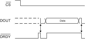 Figure 38. Using DOUT as DRDY
9.5.3 SPI Command Definitions
The ADS131E0x provides flexible configuration control. The commands, summarized in Table 9, control and configure device operation. The commands are stand-alone, except for the register read and register write operations that require a second command byte to include additional data. CS can be taken high or held low between commands but must stay low for the entire command operation (including multibyte commands). System commands and the RDATA command are decoded by the ADS131E0x on the seventh SCLK falling edge. The register read and write commands are decoded on the eighth SCLK falling edge. Be sure to follow the SPI timing requirements when pulling CS high after issuing a command.
Table 9. Command Definitions
| COMMAND | DESCRIPTION | FIRST BYTE | SECOND BYTE |
|---|---|---|---|
| SYSTEM COMMANDS | |||
| WAKEUP | Wake-up from standby mode | 0000 0010 (02h) | |
| STANDBY | Enter standby mode | 0000 0100 (04h) | |
| RESET | Reset the device | 0000 0110 (06h) | |
| START | Start or restart (synchronize) conversions | 0000 1000 (08h) | |
| STOP | Stop conversions | 0000 1010 (0Ah) | |
| OFFSETCAL | Channel offset calibration | 0001 1010 (1Ah) | |
| DATA READ COMMANDS | |||
| RDATAC | Enable read data continuous mode. This mode is the default mode at power-up.(2) |
0001 0000 (10h) | |
| SDATAC | Stop read data continuous mode | 0001 0001 (11h) | |
| RDATA | Read data by command | 0001 0010 (12h) | |
| REGISTER READ COMMANDS | |||
| RREG | Read n nnnn registers starting at address r rrrr | 001r rrrr (2xh)(1) | 000n nnnn(1) |
| WREG | Write n nnnn registers starting at address r rrrr | 010r rrrr (4xh)(1) | 000n nnnn(1) |
9.5.3.1 Sending Multibyte Commands
The ADS131E0x serial interface decodes commands in bytes and requires 4 tCLK cycles to decode and execute each command. Therefore, when sending multi-byte commands (such as RREG or WREG), a 4 tCLK period must separate the end of one byte (or command) and the next.
Assuming CLK is 2.048 MHz, then tSDECODE (4 tCLK) is 1.96 µs. When SCLK is 16 MHz, one byte can be transferred in 0.5 µs. This byte transfer time does not meet the tSDECODE specification; therefore, a delay of 1.46 µs (1.96 µs – 0.5 µs) must be inserted after the first byte and before the second byte. If SCLK is 4 MHz, one byte is transferred in 2 µs. Because this transfer time exceeds the tSDECODE specification (2 µs > 1.96 µs), the processor can send subsequent bytes without delay.
9.5.3.2 WAKEUP: Exit STANDBY Mode
The WAKEUP command exits the low-power standby mode; see the STANDBY: Enter STANDBY Mode section. Be sure to allow enough time for all circuits in standby mode to power-up (see the Electrical Characteristics table for details). There are no SCLK rate restrictions for this command and it can be issued at any time. There are no SCLK rate restrictions for this command and can be issued at any time. Any following commands must be sent after a delay of 4 tCLK cycles.
9.5.3.3 STANDBY: Enter STANDBY Mode
The STANDBY command enters low-power standby mode. All circuits in the device are powered down except for the reference section. The standby mode power consumption is specified in the Electrical Characteristics table. There are no SCLK rate restrictions for this command and can be issued at any time. Do not send any other commands other than the WAKEUP command after the device enters standby mode.
9.5.3.4 RESET: Reset Registers to Default Values
The RESET command resets the digital filter and returns all register settings to their default values; see the Reset (RESET) section for more details. There are no SCLK rate restrictions for this command and can be issued at any time. 18 tCLK cycles are required to execute the RESET command. Avoid sending any commands during this time.
9.5.3.5 START: Start Conversions
The START command starts data conversions. Tie the START pin low to control conversions by the START and STOP commands. If conversions are in progress, this command has no effect. The STOP command is used to stop conversions. If the START command is immediately followed by a STOP command, then there must be a gap of 4 tCLK cycle delay between them. The current conversion completes before further conversions are halted. There are no SCLK rate restrictions for this command and can be issued at any time.
9.5.3.6 STOP: Stop Conversions
The STOP command stops conversions. Tie the START pin low to control conversions by command. When the STOP command is sent, the conversion in progress completes and further conversions are stopped. If conversions are already stopped, this command has no effect. There are no SCLK rate restrictions for this command and can be issued at any time.
9.5.3.7 OFFSETCAL: Channel Offset Calibration
The OFFSETCAL command cancels the offset of each channel. The OFFSETCAL command is recommended to be issued every time there is a change in PGA gain settings.
When the OFFSETCAL command is issued, the device configures itself to the lowest data rate (DR[2:0] = 110, 1 kSPS) and performs the following steps for each channel:
- Short the analog inputs of each channel together and connect them to mid-supply [(AVDD + AVSS) / 2]
- Reset the digital filter (requires a filter settling time = 4 tDR)
- Collect 16 data points for calibration = 15 tDR
Total calibration time = (19 tDR × 8) + 1 ms = 153 ms.
9.5.3.8 RDATAC: Start Read Data Continuous Mode
The RDATAC command enables read data continuous mode. In this mode, conversion data are retrieved from the device without the need to issue subsequent RDATA commands. This mode places the conversion data in the output register with every DRDY falling edge so that the data can be shifted out directly with the following SCLKs. Shift out all data from the device before data are updated with a new DRDY falling edge to avoid losing data. The read data continuous mode is the device default mode; the device defaults to this mode on powerup. Figure 39 shows the ADS131E0x data output protocol when using RDATAC mode.

NOTE:
X SCLKs = (N bits)(8 channels) + 24 bits. N-bit is dependent upon the DR[2:0] registry bit settings (N = 16 or 24).RDATAC mode is cancelled by the Stop Read Data Continuous command. If the device is in RDATAC mode, a SDATAC command must be issued before any other commands can be sent to the device. There are no SCLK rate restrictions for this command. However, subsequent data retrieval SCLKs or the SDATAC command should wait at least 4 tCLK cycles before completion. RDATAC timing is shown in Figure 40. There is a keep out zone of 4 tCLK cycles around the DRDY pulse where this command cannot be issued in. If no data are retrieved from the device and CS is held low, a high-to-low DOUT transition occurs synchronously with DRDY. To retrieve data from the device after the RDATAC command is issued, make sure either the START pin is high or the START command is issued. Figure 40 shows the recommended way to use the RDATAC command. Read data continuous mode is ideally-suited for applications such as data loggers or recorders where registers are set one time and do not need to be reconfigured.

9.5.3.9 SDATAC: Stop Read Data Continuous Mode
The SDATAC command cancels the Read Data Continuous mode. There are no SCLK rate restrictions for this command, but the next command must wait for 4 tCLK cycles before completion.
9.5.3.10 RDATA: Read Data
The RDATA command loads the output shift register with the latest data when not in Read Data Continuous mode. Issue this command after DRDY goes low to read the conversion result. There are no SCLK rate restrictions for this command, and there is no wait time needed for the subsequent commands or data retrieval SCLKs. To retrieve data from the device after the RDATA command is issued, make sure either the START pin is high or the START command is issued. When reading data with the RDATA command, the read operation can overlap the next DRDY occurrence without data corruption. RDATA can be sent multiple times after new data are available, thus supporting multiple data readback. Figure 41 illustrates the recommended way to use the RDATA command. RDATA is best suited for systems where register settings must be read or the user does not have precise control over timing. Reading data using the RDATA command is recommended to avoid data corruption when the DRDY signal is not monitored.
 Figure 41. RDATA Usage
9.5.3.11 RREG: Read from Register
The RREG command reads the contents of one or more device configuration registers. The Register Read command is a two-byte command followed by the register data output. The first byte contains the command and register address. The second command byte specifies the number of registers to read – 1.
First command byte: 001r rrrr, where r rrrr is the starting register address.
Second command byte: 000n nnnn, where n nnnn is the number of registers to read – 1.
The 17th SCLK rising edge of the operation clocks out the MSB of the first register, as shown in Figure 42. When the device is in read data continuous mode, an SDATAC command must be issued before the RREG command can be issued. The RREG command can be issued any time. However, because this command is a multi-byte command, there are SCLK rate restrictions depending on how the SCLKs are issued to meet the tSDECODE timing. See the Serial Clock (SCLK) subsection of the SPI Interface section for more details. Note that CS must be low for the entire command.
 Figure 42. RREG Command Example: Read Two Registers Starting from Register 00h (ID Register)
(BYTE 1 = 0010 0000, BYTE 2 = 0000 0001)
9.5.3.12 WREG: Write to Register
The WREG command writes data to one or more device configuration registers. The Register Write command is a two-byte command followed by the register data input. The first byte contains the command and register address. The second command byte specifies the number of registers to write – 1.
First command byte: 010r rrrr, where r rrrr is the starting register address.
Second command byte: 000n nnnn, where n nnnn is the number of registers to write – 1.
After the command bytes, the register data follows (in MSB-first format), as shown in Figure 43. For multiple register writes across reserved registers (0Dh–11h), these registers must be included in the register count and the default setting of the reserved register must be written. The WREG command can be issued at any time. However, because this command is a multi-byte command, there are SCLK rate restrictions depending on how the SCLKs are issued to meet the tSDECODE timing. See the Figure 1 for more details. CS must be low for the entire command.
 Figure 43. WREG Command Example: Write Two Registers Starting from 00h (ID Register)
(BYTE 1 = 0100 0000, BYTE 2 = 0000 0001)
9.6 Register Map
Table 10 describes the various ADS131E0x registers.
Table 10. Register Map(1)
| ADDRESS | REGISTER | RESET VALUE (HEX) | BIT 7 | BIT 6 | BIT 5 | BIT 4 | BIT 3 | BIT 2 | BIT 1 | BIT 0 |
|---|---|---|---|---|---|---|---|---|---|---|
| DEVICE SETTINGS ( READ-ONLY REGISTERS) | ||||||||||
| 00h | ID | xx | REV_ID2 | REV_ID1 | REV_ID0 | 1 | 0 | 0 | NU_CH2 | NU_CH1 |
| GLOBAL SETTINGS ACROSS CHANNELS | ||||||||||
| 01h | CONFIG1 | 91 | 1 | DAISY_IN | CLK_EN | 1 | 0 | DR[2:0] | ||
| 02h | CONFIG2 | E0 | 1 | 1 | 1 | INT_TEST | 0 | TEST_AMP0 | TEST_FREQ[1:0] | |
| 03h | CONFIG3 | 40 | PDB_REFBUF | 1 | VREF_4V | 0 | OPAMP_REF | PDB_OPAMP | 0 | 0 |
| 04h | FAULT | 00 | COMP_TH[2:0] | 0 | 0 | 0 | 0 | 0 | ||
| CHANNEL-SPECIFIC SETTINGS | ||||||||||
| 05h | CH1SET | 10 | PD1 | GAIN1[2:0] | 0 | MUX1[2:0] | ||||
| 06h | CH2SET | 10 | PD2 | GAIN2[2:0] | 0 | MUX2[2:0] | ||||
| 07h | CH3SET | 10 | PD3 | GAIN3[2:0] | 0 | MUX3[2:0] | ||||
| 08h | CH4SET | 10 | PD4 | GAIN4[2:0] | 0 | MUX4[2:0] | ||||
| 09h | CH5SET | 10 | PD5 | GAIN5[2:0] | 0 | MUX5[2:0] | ||||
| 0Ah | CH6SET | 10 | PD6 | GAIN6[2:0] | 0 | MUX6[2:0] | ||||
| 0Bh | CH7SET | 10 | PD7 | GAIN7[2:0] | 0 | MUX7[2:0] | ||||
| 0Ch | CH8SET | 10 | PD8 | GAIN8[2:0] | 0 | MUX8[2:0] | ||||
| FAULT DETECT STATUS REGISTERS ( READ-ONLY REGISTERS) | ||||||||||
| 12h | FAULT_STATP | 00 | IN8P_FAULT | IN7P_FAULT | IN6P_FAULT | IN5P_FAULT | IN4P_FAULT | IN3P_FAULT | IN2P_FAULT | IN1P_FAULT |
| 13h | FAULT_STATN | 00 | IN8N_FAULT | IN7N_FAULT | IN6N_FAULT | IN5N_FAULT | IN4N_FAULT | IN3N_FAULT | IN2N_FAULT | IN1N_FAULT |
| GPIO SETTINGS | ||||||||||
| 14h | GPIO | 0F | GPIOD4 | GPIOD3 | GPIOD2 | GPIOD1 | GPIOC4 | GPIOC3 | GPIOC2 | GPIOC1 |
9.6.1 Register Descriptions
9.6.1.1 ID: ID Control Register (Factory-Programmed, Read-Only) (address = 00h) [reset = xxh]
This register is programmed during device manufacture to indicate device characteristics.
| 7 | 6 | 5 | 4 | 3 | 2 | 1 | 0 |
| REV_ID2 | REV_ID1 | REV_ID0 | 1 | 0 | 0 | NU_CH2 | NU_CH1 |
| R-1h | R-1h | R-0h | R-1h | R-0h | R-0h | R-xh | R-xh |
| LEGEND: R = Read only; -n = value after reset |
Table 11. ID: ID Control Register Field Descriptions
| Bit | Field | Type | Reset | Description |
|---|---|---|---|---|
| 7:5 | REV_ID[2:0] | R | 6h | Device family identification.
This bit indicates the device family. 110 : ADS131E0x 000, 001, 010, 011, 100, 101, 111 : Reserved |
| 4 | Reserved | R | 1h | Reserved.
Always reads 1. |
| 3:2 | Reserved | R | 0h | Reserved.
Always reads 0. |
| 1:0 | NU_CH[2:0] | R | xh | Device identification bits.
00 : 4-channel device 01 : 6-channel device 10 : 8-channel device 11 : Reserved |
9.6.1.2 CONFIG1: Configuration Register 1 (address = 01h) [reset = 91h]
This register configures daisy chain, the clock setting, and each ADC channel sample rate.
| 7 | 6 | 5 | 4 | 3 | 2 | 1 | 0 |
| 1 | DAISY_IN | CLK_EN | 1 | 0 | DR[2:0] | ||
| R/W-1h | R/W-1h | R/W-0h | R/W-1h | R/W-0h | R/W-4h | ||
| LEGEND: R/W = Read/Write; -n = value after reset |
Table 12. CONFIG1: Configuration Register 1 Field Descriptions
| Bit | Field | Type | Reset | Description |
|---|---|---|---|---|
| 7 | Reserved | R/W | 1h | Reserved.
Must be set to 1. This bit reads high. |
| 6 | DAISY_IN | R/W | 0h | Daisy-chain and multiple data readback mode.
This bit determines which mode is enabled. 0 : Daisy-chain mode 1 : Multiple data readback mode |
| 5 | CLK_EN | R/W | 0h | CLK connection(1). This bit determines if the internal oscillator signal is connected to the CLK pin when the CLKSEL pin = 1. 0 : Oscillator clock output disabled 1 : Oscillator clock output enabled |
| 4 | Reserved | R/W | 1h | Reserved.
Must be set to 1. This bit reads high. |
| 3 | Reserved | R/W | 0h | Reserved.
Must be set to 0. This bit reads low. |
| 2:0 | DR[2:0] | R/W | 1h | Output data rate.
These bits determine the output data rate and resolution; see Table 13 for details. |
Table 13. Data Rate Settings
| DR[2:0] | RESOLUTION | DATA RATE (kSPS)(1) |
|---|---|---|
| 000 | 16-bit output | 64 |
| 001 | 16-bit output | 32 (default) |
| 010 | 24-bit output | 16 |
| 011 | 24-bit output | 8 |
| 100 | 24-bit output | 4 |
| 101 | 24-bit output | 2 |
| 110 | 24-bit output | 1 |
| 111 | Do not use | NA |
9.6.1.3 CONFIG2: Configuration Register 2 (address = 02h) [reset = E0h]
This register configures the test signal generation; see the Input Multiplexer section for more details.
| 7 | 6 | 5 | 4 | 3 | 2 | 1 | 0 |
| 1 | 1 | 1 | INT_TEST | 0 | TEST_AMP | TEST_FREQ[1:0] | |
| R/W-1h | R/W-1h | R/W-1h | R/W-0h | R/W-0h | R/W-0h | R/W-0h | |
| LEGEND: R/W = Read/Write; -n = value after reset |
Table 14. CONFIG2: Configuration Register 2 Field Descriptions
| Bit | Field | Type | Reset | Description |
|---|---|---|---|---|
| 7:5 | Reserved | R/W | 7h | Reserved.
Must be set to 1. This bit reads high. |
| 4 | INT_TEST | R/W | 0h | Test signal source.
This bit determines the source for the test signal. 0 : Test signals are driven externally 1 : Test signals are generated internally |
| 3 | Reserved | R/W | 0h | Reserved.
Must be set to 0. This bit reads low. |
| 2 | TEST_AMP | R/W | 0h | Test signal amplitude.
These bits determine the calibration signal amplitude. 0 : 1 × –(VVREFP – VVREFN) / 2400 1 : 2 × –(VVREFP – VVREFN) / 2400 |
| 1:0 | TEST_FREQ[1:0] | R/W | 0h | Test signal frequency.
These bits determine the test signal frequency. 00 : Pulsed at fCLK / 221 01 : Pulsed at fCLK / 220 10 : Not used 11 : At dc |
9.6.1.4 CONFIG3: Configuration Register 3 (address = 03h) [reset = 40]
This register configures the reference and internal amplifier operation.
| 7 | 6 | 5 | 4 | 3 | 2 | 1 | 0 |
| PDB_REFBUF | 1 | VREF_4V | 0 | OPAMP_REF | PDB_OPAMP | 0 | 0 |
| R/W-0h | R/W-1h | R/W-0h | R/W-0h | R/W-0h | R/W-0h | R/W-0h | R-0h |
| LEGEND: R/W = Read/Write; -n = value after reset |
Table 15. CONFIG3: Configuration Register 3 Field Descriptions
| Bit | Field | Type | Reset | Description |
|---|---|---|---|---|
| 7 | PDB_REFBUF | R/W | 0h | PDB_REFBUF: Power-down reference buffer
This bit determines the power-down reference buffer state. 0 : Power-down internal reference buffer 1 : Enable internal reference buffer |
| 6 | Reserved | R/W | 1h | Reserved.
Must be set to 1. This bit reads high. |
| 5 | VREF_4V | R/W | 0h | Internal reference voltage.
This bit determines the internal reference voltage, VREF. 0 : VREF is set to 2.4 V 1 : VREF is set to 4 V |
| 4 | Reserved | R/W | 0h | Reserved.
Must be set to 0. This bit reads low. |
| 3 | OPAMP_REF | R/W | 0h | Op amp reference.
This bit determines whether the op amp noninverting input connects to the OPAMPP pin or to the internally-derived supply (AVDD + AVSS) / 2. 0 : Noninverting input connected to the OPAMPP pin 1 : Noninverting input connected to (AVDD + AVSS) / 2 |
| 2 | PDB_OPAMP | R/W | 0h | Op amp power-down.
This bit powers down the op amp. 0 : Power-down op amp 1 : Enable op amp |
| 1 | Reserved | R/W | 0h | Reserved.
Must be set to 0. Reads back as 0. |
| 0 | Reserved | R | 0h | Reserved.
Reads back as either 1 or 0. |
9.6.1.5 FAULT: Fault Detect Control Register (address = 04h) [reset = 00h]
This register configures the fault detection operation.
| 7 | 6 | 5 | 4 | 3 | 2 | 1 | 0 |
| COMP_TH[2:0] | 0 | 0 | 0 | 0 | 0 | ||
| R/W-0h | R/W-0h | R/W-0h | R/W-0h | R/W-0h | R/W-0h | ||
| LEGEND: R/W = Read/Write; -n = value after reset |
Table 16. FAULT: Fault Detect Control Register Field Descriptions
| Bit | Field | Type | Reset | Description |
|---|---|---|---|---|
| 7:5 | COMP_TH[2:0] | R/W | 0h | Fault detect comparator threshold.
These bits determine the fault detect comparator threshold level setting. See the Input Out-of-Range Detection section for a detailed description. Comparator high-side threshold. 000 : 95% 001 : 92.5% 010 : 90% 011 : 87.5% 100 : 85% 101 : 80% 110 : 75% 111 : 70% Comparator low-side threshold. 000 : 5% 001 : 7.5% 010 : 10% 011 : 12.5% 100 : 15% 101 : 20% 110 : 25% 111 : 30% |
| 4:0 | Reserved | R/W | 00h | Reserved.
Must be set to 0. This bit reads low. |
9.6.1.6 CHnSET: Individual Channel Settings (address = 05h to 0Ch) [reset = 10h]
This register configures the power mode, PGA gain, and multiplexer settings for the channels; see the Input Multiplexer section for details. CHnSET are similar to CH1SET, corresponding to the respective channels (see Table 10).
| 7 | 6 | 5 | 4 | 3 | 2 | 1 | 0 |
| PDn | GAINn[2:0] | 0 | MUXn[2:0] | ||||
| R/W-0h | R/W-1h | R/W-0h | R/W-0h | ||||
| LEGEND: R/W = Read/Write; -n = value after reset |
Table 17. CHnSET: Individual Channel Settings Field Descriptions
| Bit | Field | Type | Reset | Description |
|---|---|---|---|---|
| 7 | PDn | R/W | 0h | Power-down (n = individual channel number).
This bit determines the channel power mode for the corresponding channel. 0 : Normal operation 1 : Channel power-down |
| 6:4 | GAINn[2:0] | R/W | 1h | PGA gain (n = individual channel number).
These bits determine the PGA gain setting. 000 : Do not use 001 : 1 010 : 2 011 : Do not use 100 : 4 101 : 8 110 : 12 111 : Do not use |
| 3 | Reserved | R/W | 0h | Reserved.
Must be set to 0. This bit reads low. |
| 2:0 | MUXn[2:0] | R/W | 0h | Channel input (n = individual channel number).
These bits determine the channel input selection. 000 : Normal input 001 : Input shorted to (AVDD + AVSS) / 2 (for offset or noise measurements) 010 : Do not use 011 : MVDD for supply measurement 100 : Temperature sensor 101 : Test signal 110 : Do not use 111 : Do not use |
9.6.1.7 FAULT_STATP: Fault Detect Positive Input Status (address = 12h) [reset = 00h]
This register stores the status of whether the positive input on each channel has a fault or not. Faults are determined by comparing the input pin to a threshold set by Table 16; see the Input Out-of-Range Detection section for details.
| 7 | 6 | 5 | 4 | 3 | 2 | 1 | 0 |
| IN8P_FAULT | IN7P_FAULT | IN6P_FAULT | IN5P_FAULT | IN4P_FAULT | IN3P_FAULT | IN2P_FAULT | IN1P_FAULT |
| R-0h | R-0h | R-0h | R-0h | R-0h | R-0h | R-0h | R-0h |
| LEGEND: R = Read only; -n = value after reset |
Table 18. FAULT_STATP: Fault Detect Positive Input Status Field Descriptions
| Bit | Field | Type | Reset | Description |
|---|---|---|---|---|
| 7 | IN8P_FAULT | R | 0h | IN8P threshold detect.
0 : Channel 8 positive input pin does not exceed threshold set 1 : Channel 8 positive input pin exceeds threshold set |
| 6 | IN7P_FAULT | R | 0h | IN7P threshold detect.
0 : Channel 7 positive input pin does not exceed threshold set 1 : Channel 7 positive input pin exceeds threshold set |
| 5 | IN6P_FAULT | R | 0h | IN6P threshold detect.
0 : Channel 6 positive input pin does not exceed threshold set 1 : Channel 6 positive input pin exceeds threshold set |
| 4 | IN5P_FAULT | R | 0h | IN5P threshold detect.
0 : Channel 5 positive input pin does not exceed threshold set 1 : Channel 5 positive input pin exceeds threshold set |
| 3 | IN4P_FAULT | R | 0h | IN4P threshold detect.
0 : Channel 4 positive input pin does not exceed threshold set 1 : Channel 4 positive input pin exceeds threshold set |
| 2 | IN3P_FAULT | R | 0h | IN3P threshold detect.
0 : Channel 3 positive input pin does not exceed threshold set 1 : Channel 3 positive input pin exceeds threshold set |
| 1 | IN2P_FAULT | R | 0h | IN2P threshold detect.
0 : Channel 2 positive input pin does not exceed threshold set 1 : Channel 2 positive input pin exceeds threshold set |
| 0 | IN1P_FAULT | R | 0h | IN1P threshold detect.
0 : Channel 1 positive input pin does not exceed threshold set 1 : Channel 1 positive input pin exceeds threshold set |
9.6.1.8 FAULT_STATN: Fault Detect Negative Input Status (address = 13h) [reset = 00h]
This register stores the status of whether the negative input on each channel has a fault or not. Faults are determined by comparing the input pin to a threshold set by Table 16; see the Input Out-of-Range Detection section for details.
| 7 | 6 | 5 | 4 | 3 | 2 | 1 | 0 |
| IN8N_FAULT | IN7N_FAULT | IN6N_FAULT | IN5N_FAULT | IN4N_FAULT | IN3N_FAULT | IN2N_FAULT | IN1N_FAULT |
| R-0h | R-0h | R-0h | R-0h | R-0h | R-0h | R-0h | R-0h |
| LEGEND: R = Read only; -n = value after reset |
Table 19. FAULT_STATN: Fault Detect Negative Input Status Field Descriptions
| Bit | Field | Type | Reset | Description |
|---|---|---|---|---|
| 7 | IN8N_FAULT | R | 0h | IN8N threshold detect.
0 : Channel 8 negative input pin does not exceed threshold set 1 : Channel 8 negative input pin exceeds threshold set |
| 6 | IN7N_FAULT | R | 0h | IN7N threshold detect.
0 : Channel 7 negative input pin does not exceed threshold set 1 : Channel 7 negative input pin exceeds threshold set |
| 5 | IN6N_FAULT | R | 0h | IN6N threshold detect.
0 : Channel 6 negative input pin does not exceed threshold set 1 : Channel 6 negative input pin exceeds threshold set |
| 4 | IN5N_FAULT | R | 0h | IN5N threshold detect.
0 : Channel 5 negative input pin does not exceed threshold set 1 : Channel 5 negative input pin exceeds threshold set |
| 3 | IN4N_FAULT | R | 0h | IN4N threshold detect.
0 : Channel 4 negative input pin does not exceed threshold set 1 : Channel 4 negative input pin exceeds threshold set |
| 2 | IN3N_FAULT | R | 0h | IN3N threshold detect.
0 : Channel 3 negative input pin does not exceed threshold set 1 : Channel 3 negative input pin exceeds threshold set |
| 1 | IN2N_FAULT | R | 0h | IN2N threshold detect.
0 : Channel 2 negative input pin does not exceed threshold set 1 : Channel 2 negative input pin exceeds threshold set |
| 0 | IN1N_FAULT | R | 0h | IN1N threshold detect.
0 : Channel 1 negative input pin does not exceed threshold set 1 : Channel 1 negative input pin exceeds threshold set |
9.6.1.9 GPIO: General-Purpose IO Register (address = 14h) [reset = 0Fh]
This register controls the format and state of the four GPIO pins.
| 7 | 6 | 5 | 4 | 3 | 2 | 1 | 0 |
| GPIOD[4:1] | GPIOC[4:1] | ||||||
| R/W-0h | R/W-Fh | ||||||
| LEGEND: R/W = Read/Write; -n = value after reset |
Table 20. GPIO: General-Purpose IO Register Field Descriptions
| Bit | Field | Type | Reset | Description |
|---|---|---|---|---|
| 7:4 | GPIOD[4:1] | R/W | 0h | GPIO data.
These bits are used to read and write data to the GPIO ports. When reading the register, the data returned correspond to the state of the GPIO external pins, whether they are programmed as inputs or outputs. As outputs, a write to the GPIOD sets the output value. As inputs, a write to the GPIOD has no effect. |
| 3:0 | GPIOC[4:1] | R/W | Fh | GPIO control (corresponding to GPIOD).
These bits determine if the corresponding GPIOD pin is an input or output. 0 : Output 1 : Input |
