ZHCSEJ3B June 2015 – April 2020 ADS131E08S
PRODUCTION DATA.
- 1 特性
- 2 应用
- 3 说明
- 4 修订历史记录
- 5 Device Comparison
- 6 Pin Configuration and Functions
- 7 Specifications
- 8 Parameter Measurement Information
-
9 Detailed Description
- 9.1 Overview
- 9.2 Functional Block Diagram
- 9.3 Feature Description
- 9.4 Device Functional Modes
- 9.5
Programming
- 9.5.1 SPI Interface
- 9.5.2 Data Retrieval
- 9.5.3
SPI Command Definitions
- 9.5.3.1 WAKEUP: Exit STANDBY Mode
- 9.5.3.2 STANDBY: Enter STANDBY Mode
- 9.5.3.3 RESET: Reset Registers to Default Values
- 9.5.3.4 START: Start Conversions
- 9.5.3.5 STOP: Stop Conversions
- 9.5.3.6 OFFSETCAL: Channel Offset Calibration
- 9.5.3.7 RDATAC: Start Read Data Continuous Mode
- 9.5.3.8 SDATAC: Stop Read Data Continuous Mode
- 9.5.3.9 RDATA: Read Data
- 9.5.3.10 RREG: Read from Register
- 9.5.3.11 WREG: Write to Register
- 9.5.3.12 Sending Multibyte Commands
- 9.6
Register Map
- 9.6.1
Register Descriptions
- 9.6.1.1 ID: ID Control Register (Factory-Programmed, Read-Only) (address = 00h) [reset = D2h]
- 9.6.1.2 CONFIG1: Configuration Register 1 (address = 01h) [reset = 94h]
- 9.6.1.3 CONFIG2: Configuration Register 2 (address = 02h) [reset = 00h]
- 9.6.1.4 CONFIG3: Configuration Register 3 (address = 03h) [reset = E0h]
- 9.6.1.5 FAULT: Fault Detect Control Register (address = 04h) [reset = 00h]
- 9.6.1.6 CHnSET: Individual Channel Settings (address = 05h to 0Ch) [reset = 10h]
- 9.6.1.7 FAULT_STATP: Fault Detect Positive Input Status (address = 12h) [reset = 00h]
- 9.6.1.8 FAULT_STATN: Fault Detect Negative Input Status (address = 13h) [reset = 00h]
- 9.6.1.9 GPIO: General-Purpose IO Register (address = 14h) [reset = 0Fh]
- 9.6.1
Register Descriptions
- 10Application and Implementation
- 11Power Supply Recommendations
- 12Layout
- 13器件和文档支持
- 14机械、封装和可订购信息
12.2 Layout Example
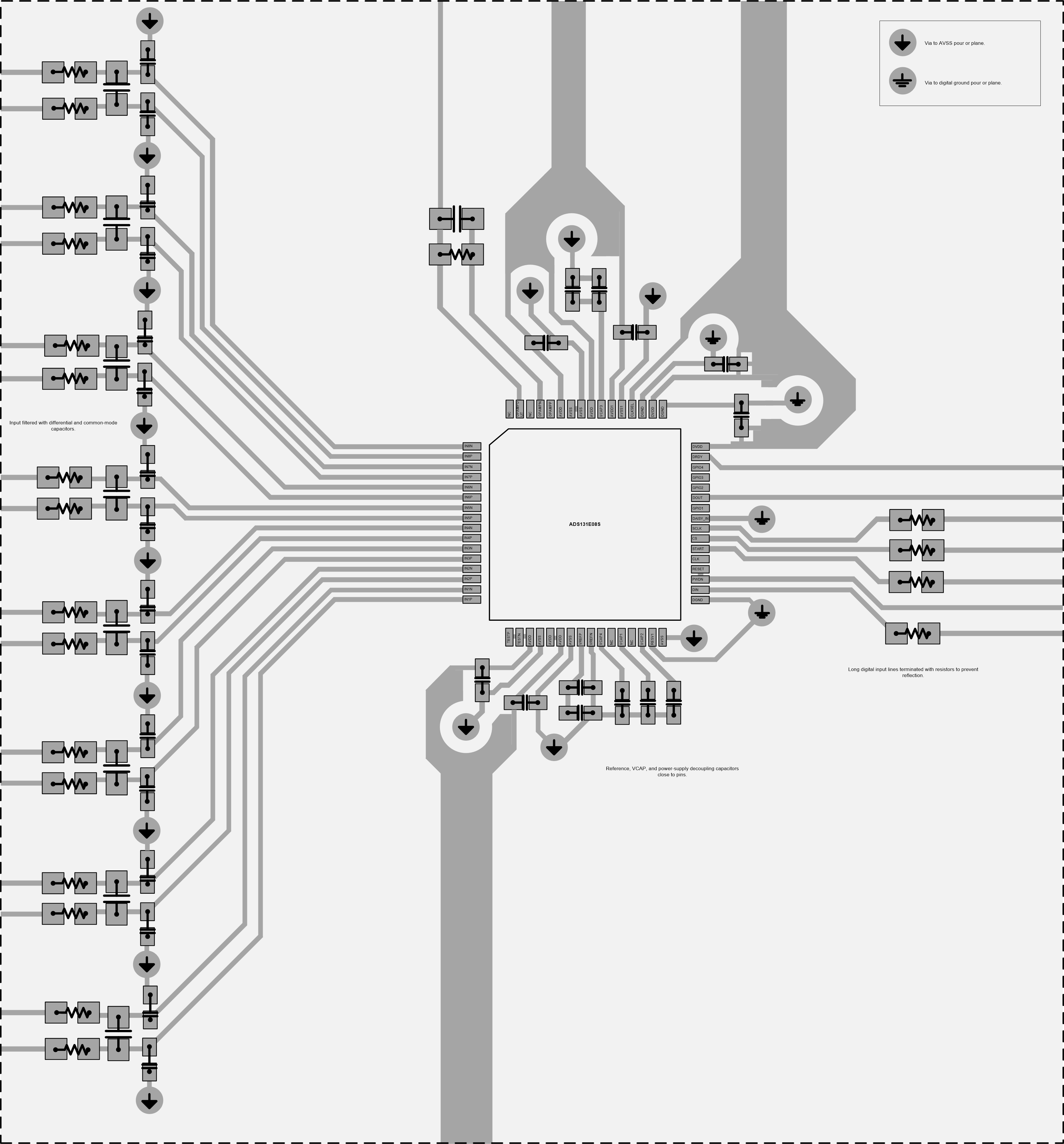
Figure 70 shows an example layout of the ADS131E08S requiring a minimum of two PCB layers. The example circuit is shown for either a unipolar analog supply connection or a bipolar analog supply connection. In this example, polygon pours are used as supply connections around the device. If a three- or four-layer PCB is used, the additional inner layers can be dedicated to route power traces. The PCB is partitioned with analog signals routed from the left, digital signals routed to the right, and power routed above and below the device.
 Figure 70. ADS131E08S Layout Example