ZHCSEJ3B June   2015  – April 2020 ADS131E08S

PRODUCTION DATA.  

  1. 特性
  2. 应用
    1.     电源应用:三相电压和电流连接
  3. 说明
  4. 修订历史记录
  5. Device Comparison
  6. Pin Configuration and Functions
    1.     Pin Functions
  7. Specifications
    1. 7.1 Absolute Maximum Ratings
    2. 7.2 ESD Ratings
    3. 7.3 Recommended Operating Conditions
    4. 7.4 Thermal Information
    5. 7.5 Electrical Characteristics
    6. 7.6 Timing Requirements
    7. 7.7 Switching Characteristics
    8. 7.8 Typical Characteristics
  8. Parameter Measurement Information
    1. 8.1 Noise Measurements
  9. Detailed Description
    1. 9.1 Overview
    2. 9.2 Functional Block Diagram
    3. 9.3 Feature Description
      1. 9.3.1  Electromagnetic Interference (EMI) Filter
      2. 9.3.2  Input Multiplexer
        1. 9.3.2.1 Device Noise Measurements
        2. 9.3.2.2 Test Signals (TestP and TestN)
        3. 9.3.2.3 Temperature Sensor (TempP, TempN)
        4. 9.3.2.4 Power-Supply Measurements (MVDDP, MVDDN)
      3. 9.3.3  Analog Input
      4. 9.3.4  PGA Settings and Input Range
        1. 9.3.4.1 Input Common-Mode Range
      5. 9.3.5  ΔΣ Modulator
      6. 9.3.6  Clock
      7. 9.3.7  Digital Decimation Filter
      8. 9.3.8  Voltage Reference
      9. 9.3.9  Input Out-of-Range Detection
      10. 9.3.10 General-Purpose Digital I/O (GPIO)
    4. 9.4 Device Functional Modes
      1. 9.4.1 Power-Down
      2. 9.4.2 Reset
      3. 9.4.3 Conversion Mode
        1. 9.4.3.1 START Pin Low-to-High Transition or START Command Sent
        2. 9.4.3.2 Input Signal Step
        3. 9.4.3.3 Continuous Conversion Mode
    5. 9.5 Programming
      1. 9.5.1 SPI Interface
        1. 9.5.1.1 Chip Select (CS)
        2. 9.5.1.2 Serial Clock (SCLK)
        3. 9.5.1.3 Data Input (DIN)
        4. 9.5.1.4 Data Output (DOUT)
        5. 9.5.1.5 Data Ready (DRDY)
      2. 9.5.2 Data Retrieval
        1. 9.5.2.1 Status Word
        2. 9.5.2.2 Readback Length
        3. 9.5.2.3 Data Format
      3. 9.5.3 SPI Command Definitions
        1. 9.5.3.1  WAKEUP: Exit STANDBY Mode
        2. 9.5.3.2  STANDBY: Enter STANDBY Mode
        3. 9.5.3.3  RESET: Reset Registers to Default Values
        4. 9.5.3.4  START: Start Conversions
        5. 9.5.3.5  STOP: Stop Conversions
        6. 9.5.3.6  OFFSETCAL: Channel Offset Calibration
        7. 9.5.3.7  RDATAC: Start Read Data Continuous Mode
        8. 9.5.3.8  SDATAC: Stop Read Data Continuous Mode
        9. 9.5.3.9  RDATA: Read Data
        10. 9.5.3.10 RREG: Read from Register
        11. 9.5.3.11 WREG: Write to Register
        12. 9.5.3.12 Sending Multibyte Commands
    6. 9.6 Register Map
      1. 9.6.1 Register Descriptions
        1. 9.6.1.1 ID: ID Control Register (Factory-Programmed, Read-Only) (address = 00h) [reset = D2h]
          1. Table 11. ID: ID Control Register Field Descriptions
        2. 9.6.1.2 CONFIG1: Configuration Register 1 (address = 01h) [reset = 94h]
          1. Table 12. CONFIG1: Configuration Register 1 Field Descriptions
        3. 9.6.1.3 CONFIG2: Configuration Register 2 (address = 02h) [reset = 00h]
          1. Table 14. CONFIG2: Configuration Register 2 Field Descriptions
        4. 9.6.1.4 CONFIG3: Configuration Register 3 (address = 03h) [reset = E0h]
          1. Table 15. CONFIG3: Configuration Register 3 Field Descriptions
        5. 9.6.1.5 FAULT: Fault Detect Control Register (address = 04h) [reset = 00h]
          1. Table 16. FAULT: Fault Detect Control Register Field Descriptions
        6. 9.6.1.6 CHnSET: Individual Channel Settings (address = 05h to 0Ch) [reset = 10h]
          1. Table 17. CHnSET: Individual Channel Settings Field Descriptions
        7. 9.6.1.7 FAULT_STATP: Fault Detect Positive Input Status (address = 12h) [reset = 00h]
          1. Table 18. FAULT_STATP: Fault Detect Positive Input Status Field Descriptions
        8. 9.6.1.8 FAULT_STATN: Fault Detect Negative Input Status (address = 13h) [reset = 00h]
          1. Table 19. FAULT_STATN: Fault Detect Negative Input Status Field Descriptions
        9. 9.6.1.9 GPIO: General-Purpose IO Register (address = 14h) [reset = 0Fh]
          1. Table 20. GPIO: General-Purpose IO Register Field Descriptions
  10. 10Application and Implementation
    1. 10.1 Application Information
      1. 10.1.1 Multiple Device Configuration
        1. 10.1.1.1 Synchronizing Multiple Devices
        2. 10.1.1.2 Standard Configuration
        3. 10.1.1.3 Daisy-Chain Configuration
      2. 10.1.2 Power Monitoring Specific Applications
      3. 10.1.3 Current Sensing
      4. 10.1.4 Voltage Sensing
    2. 10.2 Typical Application
      1. 10.2.1 Design Requirements
      2. 10.2.2 Detailed Design Procedure
      3. 10.2.3 Application Curves
    3. 10.3 Initialization Set Up
      1. 10.3.1 Setting the Device Up for Basic Data Capture
  11. 11Power Supply Recommendations
    1. 11.1 Power-Up Timing
    2. 11.2 Recommended External Capacitor Values
    3. 11.3 Device Connections for Unipolar Power Supplies
    4. 11.4 Device Connections for Bipolar Power Supplies
  12. 12Layout
    1. 12.1 Layout Guidelines
    2. 12.2 Layout Example
  13. 13器件和文档支持
    1. 13.1 文档支持
      1. 13.1.1 相关文档
    2. 13.2 支持资源
    3. 13.3 商标
    4. 13.4 静电放电警告
    5. 13.5 Glossary
  14. 14机械、封装和可订购信息

封装选项

机械数据 (封装 | 引脚)
散热焊盘机械数据 (封装 | 引脚)
订购信息

Typical Characteristics

at TA = 25°C, AVDD = 3 V, AVSS = 0 V, DVDD = 1.8 V, internal VREFP = 2.4 V, VREFN = AVSS, external fCLK = 2.048 MHz, data rate = 8 kSPS, and gain = 1 (unless otherwise noted)
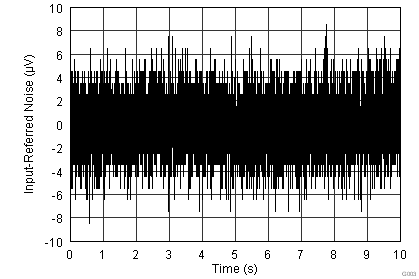
ADS131E08S G003_SBAS705.png
Data rate = 1 kSPS, gain = 1
Figure 3. Input-Referred Noise
ADS131E08S G005_SBAS705.png
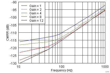
Data rate = 4 kSPS, VIN = AVDD – 0.3 V to AVSS + 0.3 V
Figure 5. Common-Mode Rejection Ratio vs Frequency
ADS131E08S G007_SBAS705.png
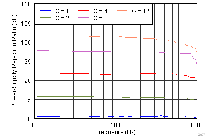
Figure 7. PSRR vs Frequency
ADS131E08S G009_SBAS705.png
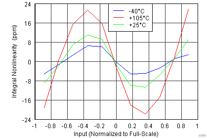
Figure 9. INL vs Temperature
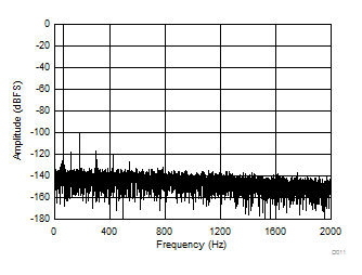
ADS131E08S D011_sbas705.gif
Gain = 1, THD = –100 dB, SNR = 107 dB,
data rate = 4 kSPS, 16384 points
Figure 11. THD FFT Plot
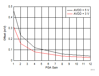
ADS131E08S D012_sbas705.gif
Figure 13. Offset vs PGA Gain (Absolute Value)
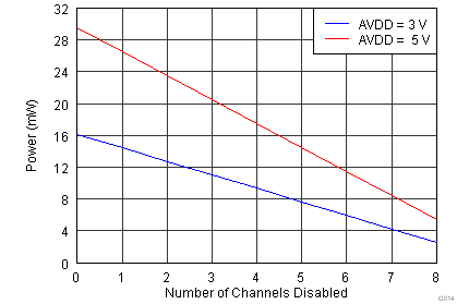
ADS131E08S G014_SBAS705.png
Figure 15. Channel Power
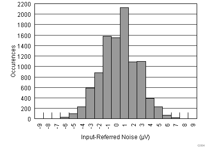
ADS131E08S G004_SBAS705.png
Data rate = 1 kSPS, gain = 1
Figure 4. Noise Histogram
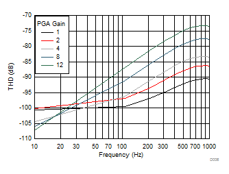
ADS131E08S D006_sbas705.gif
Figure 6. Total Harmonic Distortion vs Frequency
ADS131E08S G008_SBAS705.png
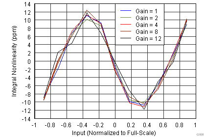
Figure 8. INL vs PGA Gain
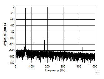
ADS131E08S D010_sbas705.gif
Gain = 1, THD = –101.5 dB, SNR = 111 dB,
data rate = 1 kSPS, 16384 points
Figure 10. THD FFT Plot
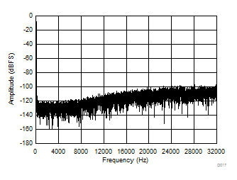
ADS131E08S D017_sbas705.gif
Gain = 1, THD = –100 dB, SNR = 76 dB,
data rate = 64 kSPS, 16384 points
Figure 12. FFT Plot
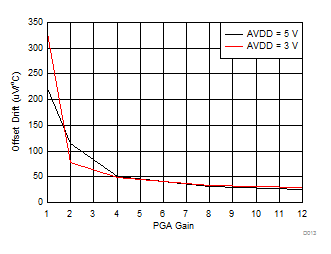
ADS131E08S D013_sbas705.gif
Figure 14. Offset Drift vs PGA Gain
ADS131E08S D015_sbas705.gif
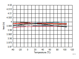
AVDD = 5 V, AVSS = 0 V, VREF = 4 V
Figure 16. Internal VREF vs Temperature