ZHCSEJ3B June 2015 – April 2020 ADS131E08S
PRODUCTION DATA.
- 1 特性
- 2 应用
- 3 说明
- 4 修订历史记录
- 5 Device Comparison
- 6 Pin Configuration and Functions
- 7 Specifications
- 8 Parameter Measurement Information
-
9 Detailed Description
- 9.1 Overview
- 9.2 Functional Block Diagram
- 9.3 Feature Description
- 9.4 Device Functional Modes
- 9.5
Programming
- 9.5.1 SPI Interface
- 9.5.2 Data Retrieval
- 9.5.3
SPI Command Definitions
- 9.5.3.1 WAKEUP: Exit STANDBY Mode
- 9.5.3.2 STANDBY: Enter STANDBY Mode
- 9.5.3.3 RESET: Reset Registers to Default Values
- 9.5.3.4 START: Start Conversions
- 9.5.3.5 STOP: Stop Conversions
- 9.5.3.6 OFFSETCAL: Channel Offset Calibration
- 9.5.3.7 RDATAC: Start Read Data Continuous Mode
- 9.5.3.8 SDATAC: Stop Read Data Continuous Mode
- 9.5.3.9 RDATA: Read Data
- 9.5.3.10 RREG: Read from Register
- 9.5.3.11 WREG: Write to Register
- 9.5.3.12 Sending Multibyte Commands
- 9.6
Register Map
- 9.6.1
Register Descriptions
- 9.6.1.1 ID: ID Control Register (Factory-Programmed, Read-Only) (address = 00h) [reset = D2h]
- 9.6.1.2 CONFIG1: Configuration Register 1 (address = 01h) [reset = 94h]
- 9.6.1.3 CONFIG2: Configuration Register 2 (address = 02h) [reset = 00h]
- 9.6.1.4 CONFIG3: Configuration Register 3 (address = 03h) [reset = E0h]
- 9.6.1.5 FAULT: Fault Detect Control Register (address = 04h) [reset = 00h]
- 9.6.1.6 CHnSET: Individual Channel Settings (address = 05h to 0Ch) [reset = 10h]
- 9.6.1.7 FAULT_STATP: Fault Detect Positive Input Status (address = 12h) [reset = 00h]
- 9.6.1.8 FAULT_STATN: Fault Detect Negative Input Status (address = 13h) [reset = 00h]
- 9.6.1.9 GPIO: General-Purpose IO Register (address = 14h) [reset = 0Fh]
- 9.6.1
Register Descriptions
- 10Application and Implementation
- 11Power Supply Recommendations
- 12Layout
- 13器件和文档支持
- 14机械、封装和可订购信息
9.3.3 Analog Input
The analog inputs to the device connect directly to an integrated low-noise, low-drift, high input impedance, programmable gain amplifier. The amplifier is located following the individual channel multiplexer.
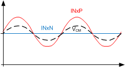
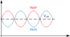
The ADS131E08S analog inputs are fully differential. The differential input voltage (VINxP – VINxN) can span from –VREF / gain to VREF / gain. See the Data Format section for an explanation of the correlation between the analog input and digital codes. There are two general methods of driving the ADS131E08S analog inputs: pseudo-differential or fully-differential, as shown in Figure 19, Figure 20, and Figure 21.
 Figure 19. Methods of Driving the ADS131E08S: Pseudo-Differential or Fully Differential
  Figure 20. Pseudo-Differential Input Mode
  Figure 21. Fully-Differential Input Mode
 Hold the INxN pin at a common voltage, preferably at mid supply, to configure the fully differential input for a pseudo-differential signal. Swing the INxP pin around the common voltage –VREF / gain to VREF / gain and remain within the absolute maximum specifications. Verify that the differential signal at the minimum and maximum points meets the common-mode input specification discussed in the Input Common-Mode Range section.
Configure the signals at INxP and INxN to be 180° out-of-phase centered around a common voltage to use a fully-differential input method. Both the INxP and INxN inputs swing from the common voltage + ½ VREF / gain to the common voltage – ½ VREF / gain. The differential voltage at the maximum and minimum points is equal to –VREF / gain to VREF / gain. Use the ADS131E08S in a differential configuration to maximize the dynamic range of the data converter. For optimal performance, the common voltage is recommended to be set at the midpoint of the analog supplies [(AVDD + AVSS) / 2].
If any of the analog input channels are not used, then power-down these pins using register bits to conserve power. See the SPI Command Definitions section for more information on how to power-down individual channels. Tie any unused or powered down analog input pins directly to AVDD.