ZHCSEJ3B June   2015  – April 2020 ADS131E08S

PRODUCTION DATA.  

  1. 特性
  2. 应用
    1.     电源应用:三相电压和电流连接
  3. 说明
  4. 修订历史记录
  5. Device Comparison
  6. Pin Configuration and Functions
    1.     Pin Functions
  7. Specifications
    1. 7.1 Absolute Maximum Ratings
    2. 7.2 ESD Ratings
    3. 7.3 Recommended Operating Conditions
    4. 7.4 Thermal Information
    5. 7.5 Electrical Characteristics
    6. 7.6 Timing Requirements
    7. 7.7 Switching Characteristics
    8. 7.8 Typical Characteristics
  8. Parameter Measurement Information
    1. 8.1 Noise Measurements
  9. Detailed Description
    1. 9.1 Overview
    2. 9.2 Functional Block Diagram
    3. 9.3 Feature Description
      1. 9.3.1  Electromagnetic Interference (EMI) Filter
      2. 9.3.2  Input Multiplexer
        1. 9.3.2.1 Device Noise Measurements
        2. 9.3.2.2 Test Signals (TestP and TestN)
        3. 9.3.2.3 Temperature Sensor (TempP, TempN)
        4. 9.3.2.4 Power-Supply Measurements (MVDDP, MVDDN)
      3. 9.3.3  Analog Input
      4. 9.3.4  PGA Settings and Input Range
        1. 9.3.4.1 Input Common-Mode Range
      5. 9.3.5  ΔΣ Modulator
      6. 9.3.6  Clock
      7. 9.3.7  Digital Decimation Filter
      8. 9.3.8  Voltage Reference
      9. 9.3.9  Input Out-of-Range Detection
      10. 9.3.10 General-Purpose Digital I/O (GPIO)
    4. 9.4 Device Functional Modes
      1. 9.4.1 Power-Down
      2. 9.4.2 Reset
      3. 9.4.3 Conversion Mode
        1. 9.4.3.1 START Pin Low-to-High Transition or START Command Sent
        2. 9.4.3.2 Input Signal Step
        3. 9.4.3.3 Continuous Conversion Mode
    5. 9.5 Programming
      1. 9.5.1 SPI Interface
        1. 9.5.1.1 Chip Select (CS)
        2. 9.5.1.2 Serial Clock (SCLK)
        3. 9.5.1.3 Data Input (DIN)
        4. 9.5.1.4 Data Output (DOUT)
        5. 9.5.1.5 Data Ready (DRDY)
      2. 9.5.2 Data Retrieval
        1. 9.5.2.1 Status Word
        2. 9.5.2.2 Readback Length
        3. 9.5.2.3 Data Format
      3. 9.5.3 SPI Command Definitions
        1. 9.5.3.1  WAKEUP: Exit STANDBY Mode
        2. 9.5.3.2  STANDBY: Enter STANDBY Mode
        3. 9.5.3.3  RESET: Reset Registers to Default Values
        4. 9.5.3.4  START: Start Conversions
        5. 9.5.3.5  STOP: Stop Conversions
        6. 9.5.3.6  OFFSETCAL: Channel Offset Calibration
        7. 9.5.3.7  RDATAC: Start Read Data Continuous Mode
        8. 9.5.3.8  SDATAC: Stop Read Data Continuous Mode
        9. 9.5.3.9  RDATA: Read Data
        10. 9.5.3.10 RREG: Read from Register
        11. 9.5.3.11 WREG: Write to Register
        12. 9.5.3.12 Sending Multibyte Commands
    6. 9.6 Register Map
      1. 9.6.1 Register Descriptions
        1. 9.6.1.1 ID: ID Control Register (Factory-Programmed, Read-Only) (address = 00h) [reset = D2h]
          1. Table 11. ID: ID Control Register Field Descriptions
        2. 9.6.1.2 CONFIG1: Configuration Register 1 (address = 01h) [reset = 94h]
          1. Table 12. CONFIG1: Configuration Register 1 Field Descriptions
        3. 9.6.1.3 CONFIG2: Configuration Register 2 (address = 02h) [reset = 00h]
          1. Table 14. CONFIG2: Configuration Register 2 Field Descriptions
        4. 9.6.1.4 CONFIG3: Configuration Register 3 (address = 03h) [reset = E0h]
          1. Table 15. CONFIG3: Configuration Register 3 Field Descriptions
        5. 9.6.1.5 FAULT: Fault Detect Control Register (address = 04h) [reset = 00h]
          1. Table 16. FAULT: Fault Detect Control Register Field Descriptions
        6. 9.6.1.6 CHnSET: Individual Channel Settings (address = 05h to 0Ch) [reset = 10h]
          1. Table 17. CHnSET: Individual Channel Settings Field Descriptions
        7. 9.6.1.7 FAULT_STATP: Fault Detect Positive Input Status (address = 12h) [reset = 00h]
          1. Table 18. FAULT_STATP: Fault Detect Positive Input Status Field Descriptions
        8. 9.6.1.8 FAULT_STATN: Fault Detect Negative Input Status (address = 13h) [reset = 00h]
          1. Table 19. FAULT_STATN: Fault Detect Negative Input Status Field Descriptions
        9. 9.6.1.9 GPIO: General-Purpose IO Register (address = 14h) [reset = 0Fh]
          1. Table 20. GPIO: General-Purpose IO Register Field Descriptions
  10. 10Application and Implementation
    1. 10.1 Application Information
      1. 10.1.1 Multiple Device Configuration
        1. 10.1.1.1 Synchronizing Multiple Devices
        2. 10.1.1.2 Standard Configuration
        3. 10.1.1.3 Daisy-Chain Configuration
      2. 10.1.2 Power Monitoring Specific Applications
      3. 10.1.3 Current Sensing
      4. 10.1.4 Voltage Sensing
    2. 10.2 Typical Application
      1. 10.2.1 Design Requirements
      2. 10.2.2 Detailed Design Procedure
      3. 10.2.3 Application Curves
    3. 10.3 Initialization Set Up
      1. 10.3.1 Setting the Device Up for Basic Data Capture
  11. 11Power Supply Recommendations
    1. 11.1 Power-Up Timing
    2. 11.2 Recommended External Capacitor Values
    3. 11.3 Device Connections for Unipolar Power Supplies
    4. 11.4 Device Connections for Bipolar Power Supplies
  12. 12Layout
    1. 12.1 Layout Guidelines
    2. 12.2 Layout Example
  13. 13器件和文档支持
    1. 13.1 文档支持
      1. 13.1.1 相关文档
    2. 13.2 支持资源
    3. 13.3 商标
    4. 13.4 静电放电警告
    5. 13.5 Glossary
  14. 14机械、封装和可订购信息

封装选项

机械数据 (封装 | 引脚)
散热焊盘机械数据 (封装 | 引脚)
订购信息

PGA Settings and Input Range

Each channel has its own configurable programmable gain amplifier (PGA) following its multiplexer. The PGA is designed using two operational amplifiers in a differential configuration, as shown in Figure 22. Set the gain to one of five settings (1, 2, 4, 8, and 12) using the CHnSET registers for each individual channel (see the CHnSET registers in the Register Map section for details). The ADS131E08S has CMOS inputs and therefore has negligible current noise. Table 3 shows the typical small-signal bandwidth values for various gain settings.
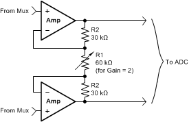
ADS131E08S ai_pga_implement_sbas705.gifFigure 22. PGA Implementation

Table 3. PGA Gain versus Bandwidth

GAIN NOMINAL BANDWIDTH AT TA = 25°C (kHz)
1 237
2 146
4 96
8 48
12 32

The PGA resistor string that implements the gain has 120 kΩ of resistance for a gain of 2. This resistance provides a current path across the PGA outputs in the presence of a differential input signal. This current is in addition to the quiescent current specified for the device in the presence of a differential signal at the input.