ZHCSEJ3B June   2015  – April 2020 ADS131E08S

PRODUCTION DATA.  

  1. 特性
  2. 应用
    1.     电源应用:三相电压和电流连接
  3. 说明
  4. 修订历史记录
  5. Device Comparison
  6. Pin Configuration and Functions
    1.     Pin Functions
  7. Specifications
    1. 7.1 Absolute Maximum Ratings
    2. 7.2 ESD Ratings
    3. 7.3 Recommended Operating Conditions
    4. 7.4 Thermal Information
    5. 7.5 Electrical Characteristics
    6. 7.6 Timing Requirements
    7. 7.7 Switching Characteristics
    8. 7.8 Typical Characteristics
  8. Parameter Measurement Information
    1. 8.1 Noise Measurements
  9. Detailed Description
    1. 9.1 Overview
    2. 9.2 Functional Block Diagram
    3. 9.3 Feature Description
      1. 9.3.1  Electromagnetic Interference (EMI) Filter
      2. 9.3.2  Input Multiplexer
        1. 9.3.2.1 Device Noise Measurements
        2. 9.3.2.2 Test Signals (TestP and TestN)
        3. 9.3.2.3 Temperature Sensor (TempP, TempN)
        4. 9.3.2.4 Power-Supply Measurements (MVDDP, MVDDN)
      3. 9.3.3  Analog Input
      4. 9.3.4  PGA Settings and Input Range
        1. 9.3.4.1 Input Common-Mode Range
      5. 9.3.5  ΔΣ Modulator
      6. 9.3.6  Clock
      7. 9.3.7  Digital Decimation Filter
      8. 9.3.8  Voltage Reference
      9. 9.3.9  Input Out-of-Range Detection
      10. 9.3.10 General-Purpose Digital I/O (GPIO)
    4. 9.4 Device Functional Modes
      1. 9.4.1 Power-Down
      2. 9.4.2 Reset
      3. 9.4.3 Conversion Mode
        1. 9.4.3.1 START Pin Low-to-High Transition or START Command Sent
        2. 9.4.3.2 Input Signal Step
        3. 9.4.3.3 Continuous Conversion Mode
    5. 9.5 Programming
      1. 9.5.1 SPI Interface
        1. 9.5.1.1 Chip Select (CS)
        2. 9.5.1.2 Serial Clock (SCLK)
        3. 9.5.1.3 Data Input (DIN)
        4. 9.5.1.4 Data Output (DOUT)
        5. 9.5.1.5 Data Ready (DRDY)
      2. 9.5.2 Data Retrieval
        1. 9.5.2.1 Status Word
        2. 9.5.2.2 Readback Length
        3. 9.5.2.3 Data Format
      3. 9.5.3 SPI Command Definitions
        1. 9.5.3.1  WAKEUP: Exit STANDBY Mode
        2. 9.5.3.2  STANDBY: Enter STANDBY Mode
        3. 9.5.3.3  RESET: Reset Registers to Default Values
        4. 9.5.3.4  START: Start Conversions
        5. 9.5.3.5  STOP: Stop Conversions
        6. 9.5.3.6  OFFSETCAL: Channel Offset Calibration
        7. 9.5.3.7  RDATAC: Start Read Data Continuous Mode
        8. 9.5.3.8  SDATAC: Stop Read Data Continuous Mode
        9. 9.5.3.9  RDATA: Read Data
        10. 9.5.3.10 RREG: Read from Register
        11. 9.5.3.11 WREG: Write to Register
        12. 9.5.3.12 Sending Multibyte Commands
    6. 9.6 Register Map
      1. 9.6.1 Register Descriptions
        1. 9.6.1.1 ID: ID Control Register (Factory-Programmed, Read-Only) (address = 00h) [reset = D2h]
          1. Table 11. ID: ID Control Register Field Descriptions
        2. 9.6.1.2 CONFIG1: Configuration Register 1 (address = 01h) [reset = 94h]
          1. Table 12. CONFIG1: Configuration Register 1 Field Descriptions
        3. 9.6.1.3 CONFIG2: Configuration Register 2 (address = 02h) [reset = 00h]
          1. Table 14. CONFIG2: Configuration Register 2 Field Descriptions
        4. 9.6.1.4 CONFIG3: Configuration Register 3 (address = 03h) [reset = E0h]
          1. Table 15. CONFIG3: Configuration Register 3 Field Descriptions
        5. 9.6.1.5 FAULT: Fault Detect Control Register (address = 04h) [reset = 00h]
          1. Table 16. FAULT: Fault Detect Control Register Field Descriptions
        6. 9.6.1.6 CHnSET: Individual Channel Settings (address = 05h to 0Ch) [reset = 10h]
          1. Table 17. CHnSET: Individual Channel Settings Field Descriptions
        7. 9.6.1.7 FAULT_STATP: Fault Detect Positive Input Status (address = 12h) [reset = 00h]
          1. Table 18. FAULT_STATP: Fault Detect Positive Input Status Field Descriptions
        8. 9.6.1.8 FAULT_STATN: Fault Detect Negative Input Status (address = 13h) [reset = 00h]
          1. Table 19. FAULT_STATN: Fault Detect Negative Input Status Field Descriptions
        9. 9.6.1.9 GPIO: General-Purpose IO Register (address = 14h) [reset = 0Fh]
          1. Table 20. GPIO: General-Purpose IO Register Field Descriptions
  10. 10Application and Implementation
    1. 10.1 Application Information
      1. 10.1.1 Multiple Device Configuration
        1. 10.1.1.1 Synchronizing Multiple Devices
        2. 10.1.1.2 Standard Configuration
        3. 10.1.1.3 Daisy-Chain Configuration
      2. 10.1.2 Power Monitoring Specific Applications
      3. 10.1.3 Current Sensing
      4. 10.1.4 Voltage Sensing
    2. 10.2 Typical Application
      1. 10.2.1 Design Requirements
      2. 10.2.2 Detailed Design Procedure
      3. 10.2.3 Application Curves
    3. 10.3 Initialization Set Up
      1. 10.3.1 Setting the Device Up for Basic Data Capture
  11. 11Power Supply Recommendations
    1. 11.1 Power-Up Timing
    2. 11.2 Recommended External Capacitor Values
    3. 11.3 Device Connections for Unipolar Power Supplies
    4. 11.4 Device Connections for Bipolar Power Supplies
  12. 12Layout
    1. 12.1 Layout Guidelines
    2. 12.2 Layout Example
  13. 13器件和文档支持
    1. 13.1 文档支持
      1. 13.1.1 相关文档
    2. 13.2 支持资源
    3. 13.3 商标
    4. 13.4 静电放电警告
    5. 13.5 Glossary
  14. 14机械、封装和可订购信息

封装选项

机械数据 (封装 | 引脚)
散热焊盘机械数据 (封装 | 引脚)
订购信息

Data Ready (DRDY)

DRDY is an output signal that transitions from high to low to indicate that new conversion data are ready. DRDY behavior is determined by whether the device is in RDATAC mode or if the RDATA command is being used to read data on demand. See the RDATAC: Start Read Data Continuous Mode and RDATA: Read Data sections for further details. The CS signal has no effect on the data-ready signal.

When reading data with the RDATA command, the read operation can overlap the next DRDY occurrence without data corruption.

Figure 37 shows the relationship between DRDY, DOUT, and SCLK during data retrieval. DOUT transitions on the SCLK rising edge. DRDY goes high on the first SCLK falling edge regardless of whether data are being retrieved from the device or a command is being sent through the DIN pin. Data starts with the MSB of the status word and then proceeds to the ADC channel data in sequential order (channel 1, channel 2, and so forth). Data for powered down channels appear in the data stream as 0s and are to be ignored.
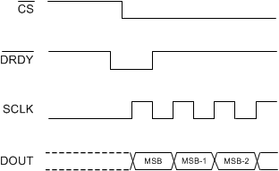
ADS131E08S DRDY_dataretrieval_sbas459.gifFigure 37. DRDY Behavior with Data Retrieval

The DRDY signal is cleared on the first SCLK falling edge regardless of the state of CS. This condition must be taken into consideration if the SPI bus is used to communicate with other devices on the same bus. Figure 38 shows a behavior diagram for DRDY when SCLKs are sent with CS high. Figure 38 shows that no data are clocked out, but the DRDY signal is cleared.

ADS131E08S DRDYSCLK_behavior_sbas459.gifFigure 38. DRDY and SCLK Behavior when CS is High