ZHCSEJ3B June   2015  – April 2020 ADS131E08S

PRODUCTION DATA.  

  1. 特性
  2. 应用
    1.     电源应用:三相电压和电流连接
  3. 说明
  4. 修订历史记录
  5. Device Comparison
  6. Pin Configuration and Functions
    1.     Pin Functions
  7. Specifications
    1. 7.1 Absolute Maximum Ratings
    2. 7.2 ESD Ratings
    3. 7.3 Recommended Operating Conditions
    4. 7.4 Thermal Information
    5. 7.5 Electrical Characteristics
    6. 7.6 Timing Requirements
    7. 7.7 Switching Characteristics
    8. 7.8 Typical Characteristics
  8. Parameter Measurement Information
    1. 8.1 Noise Measurements
  9. Detailed Description
    1. 9.1 Overview
    2. 9.2 Functional Block Diagram
    3. 9.3 Feature Description
      1. 9.3.1  Electromagnetic Interference (EMI) Filter
      2. 9.3.2  Input Multiplexer
        1. 9.3.2.1 Device Noise Measurements
        2. 9.3.2.2 Test Signals (TestP and TestN)
        3. 9.3.2.3 Temperature Sensor (TempP, TempN)
        4. 9.3.2.4 Power-Supply Measurements (MVDDP, MVDDN)
      3. 9.3.3  Analog Input
      4. 9.3.4  PGA Settings and Input Range
        1. 9.3.4.1 Input Common-Mode Range
      5. 9.3.5  ΔΣ Modulator
      6. 9.3.6  Clock
      7. 9.3.7  Digital Decimation Filter
      8. 9.3.8  Voltage Reference
      9. 9.3.9  Input Out-of-Range Detection
      10. 9.3.10 General-Purpose Digital I/O (GPIO)
    4. 9.4 Device Functional Modes
      1. 9.4.1 Power-Down
      2. 9.4.2 Reset
      3. 9.4.3 Conversion Mode
        1. 9.4.3.1 START Pin Low-to-High Transition or START Command Sent
        2. 9.4.3.2 Input Signal Step
        3. 9.4.3.3 Continuous Conversion Mode
    5. 9.5 Programming
      1. 9.5.1 SPI Interface
        1. 9.5.1.1 Chip Select (CS)
        2. 9.5.1.2 Serial Clock (SCLK)
        3. 9.5.1.3 Data Input (DIN)
        4. 9.5.1.4 Data Output (DOUT)
        5. 9.5.1.5 Data Ready (DRDY)
      2. 9.5.2 Data Retrieval
        1. 9.5.2.1 Status Word
        2. 9.5.2.2 Readback Length
        3. 9.5.2.3 Data Format
      3. 9.5.3 SPI Command Definitions
        1. 9.5.3.1  WAKEUP: Exit STANDBY Mode
        2. 9.5.3.2  STANDBY: Enter STANDBY Mode
        3. 9.5.3.3  RESET: Reset Registers to Default Values
        4. 9.5.3.4  START: Start Conversions
        5. 9.5.3.5  STOP: Stop Conversions
        6. 9.5.3.6  OFFSETCAL: Channel Offset Calibration
        7. 9.5.3.7  RDATAC: Start Read Data Continuous Mode
        8. 9.5.3.8  SDATAC: Stop Read Data Continuous Mode
        9. 9.5.3.9  RDATA: Read Data
        10. 9.5.3.10 RREG: Read from Register
        11. 9.5.3.11 WREG: Write to Register
        12. 9.5.3.12 Sending Multibyte Commands
    6. 9.6 Register Map
      1. 9.6.1 Register Descriptions
        1. 9.6.1.1 ID: ID Control Register (Factory-Programmed, Read-Only) (address = 00h) [reset = D2h]
          1. Table 11. ID: ID Control Register Field Descriptions
        2. 9.6.1.2 CONFIG1: Configuration Register 1 (address = 01h) [reset = 94h]
          1. Table 12. CONFIG1: Configuration Register 1 Field Descriptions
        3. 9.6.1.3 CONFIG2: Configuration Register 2 (address = 02h) [reset = 00h]
          1. Table 14. CONFIG2: Configuration Register 2 Field Descriptions
        4. 9.6.1.4 CONFIG3: Configuration Register 3 (address = 03h) [reset = E0h]
          1. Table 15. CONFIG3: Configuration Register 3 Field Descriptions
        5. 9.6.1.5 FAULT: Fault Detect Control Register (address = 04h) [reset = 00h]
          1. Table 16. FAULT: Fault Detect Control Register Field Descriptions
        6. 9.6.1.6 CHnSET: Individual Channel Settings (address = 05h to 0Ch) [reset = 10h]
          1. Table 17. CHnSET: Individual Channel Settings Field Descriptions
        7. 9.6.1.7 FAULT_STATP: Fault Detect Positive Input Status (address = 12h) [reset = 00h]
          1. Table 18. FAULT_STATP: Fault Detect Positive Input Status Field Descriptions
        8. 9.6.1.8 FAULT_STATN: Fault Detect Negative Input Status (address = 13h) [reset = 00h]
          1. Table 19. FAULT_STATN: Fault Detect Negative Input Status Field Descriptions
        9. 9.6.1.9 GPIO: General-Purpose IO Register (address = 14h) [reset = 0Fh]
          1. Table 20. GPIO: General-Purpose IO Register Field Descriptions
  10. 10Application and Implementation
    1. 10.1 Application Information
      1. 10.1.1 Multiple Device Configuration
        1. 10.1.1.1 Synchronizing Multiple Devices
        2. 10.1.1.2 Standard Configuration
        3. 10.1.1.3 Daisy-Chain Configuration
      2. 10.1.2 Power Monitoring Specific Applications
      3. 10.1.3 Current Sensing
      4. 10.1.4 Voltage Sensing
    2. 10.2 Typical Application
      1. 10.2.1 Design Requirements
      2. 10.2.2 Detailed Design Procedure
      3. 10.2.3 Application Curves
    3. 10.3 Initialization Set Up
      1. 10.3.1 Setting the Device Up for Basic Data Capture
  11. 11Power Supply Recommendations
    1. 11.1 Power-Up Timing
    2. 11.2 Recommended External Capacitor Values
    3. 11.3 Device Connections for Unipolar Power Supplies
    4. 11.4 Device Connections for Bipolar Power Supplies
  12. 12Layout
    1. 12.1 Layout Guidelines
    2. 12.2 Layout Example
  13. 13器件和文档支持
    1. 13.1 文档支持
      1. 13.1.1 相关文档
    2. 13.2 支持资源
    3. 13.3 商标
    4. 13.4 静电放电警告
    5. 13.5 Glossary
  14. 14机械、封装和可订购信息

封装选项

机械数据 (封装 | 引脚)
散热焊盘机械数据 (封装 | 引脚)
订购信息

Voltage Sensing

Figure 59 illustrates a simplified diagram of commonly-used differential and single-ended methods of voltage sensing. A resistor divider network is used to step down the line voltage to within the acceptable ADS131E08S input range and then connect to the inputs (INxP and INxN) through an antialiasing RC filter formed by resistor R3 and capacitor C. The common-mode bias voltage [(AVDD + AVSS) / 2] can be obtained from the ADS131E08S by either configuring the internal op amp in a unity-gain configuration using the RF resistor and setting the OPAMP_REF bit of the CONFIG3 register, or generated externally by using a resistor divider network between the positive and negative supplies.

In either of the cases illustrated in Figure 59 (Figure 59a for a differential input and Figure 59b for a single-ended input), the line voltage is divided down by a factor of [R2 / (R1 + R2)]. Values of R1 and R2 must be carefully chosen so that the voltage across the ADS131E08S inputs (INxP and INxN) does not exceed the range of the ADS131E08S over the full operating dynamic range. Use separate external op amps to source and sink current because the internal op amp has very limited current sink and source capability. Additionally, separate op amps for each channel help isolate individual phases from one another to limit crosstalk.
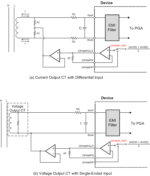
ADS131E08S ai_simple_isense_conex_bas705.gifFigure 58. Simplified Current-Sensing Connections
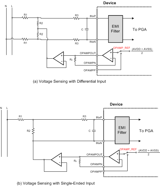
ADS131E08S ai_simple_vsense_conex_bas705.gifFigure 59. Simplified Voltage-Sensing Connections