ZHCSOL6 August 2022 ADS131M02-Q1
PRODUCTION DATA
- 1 Features
- 2 Applications
- 3 Description
- 4 Revision History
- 5 Pin Configuration and Functions
- 6 Specifications
- 7 Parameter Measurement Information
-
8 Detailed Description
- 8.1 Overview
- 8.2 Functional Block Diagram
- 8.3
Feature Description
- 8.3.1 Input ESD Protection Circuitry
- 8.3.2 Input Multiplexer
- 8.3.3 Programmable Gain Amplifier (PGA)
- 8.3.4 Voltage Reference
- 8.3.5 Clocking and Power Modes
- 8.3.6 ΔΣ Modulator
- 8.3.7 Digital Filter
- 8.3.8 DC Block Filter
- 8.3.9 Internal Test Signals
- 8.3.10 Channel Phase Calibration
- 8.3.11 Calibration Registers
- 8.3.12 Communication Cyclic Redundancy Check (CRC)
- 8.3.13 Register Map CRC
- 8.4 Device Functional Modes
- 8.5
Programming
- 8.5.1
Interface
- 8.5.1.1 Chip Select (CS)
- 8.5.1.2 Serial Data Clock (SCLK)
- 8.5.1.3 Serial Data Input (DIN)
- 8.5.1.4 Serial Data Output (DOUT)
- 8.5.1.5 Data Ready (DRDY)
- 8.5.1.6 Conversion Synchronization or System Reset (SYNC/RESET)
- 8.5.1.7 SPI Communication Frames
- 8.5.1.8 SPI Communication Words
- 8.5.1.9 ADC Conversion Data
- 8.5.1.10
Commands
- 8.5.1.10.1 NULL (0000 0000 0000 0000)
- 8.5.1.10.2 RESET (0000 0000 0001 0001)
- 8.5.1.10.3 STANDBY (0000 0000 0010 0010)
- 8.5.1.10.4 WAKEUP (0000 0000 0011 0011)
- 8.5.1.10.5 LOCK (0000 0101 0101 0101)
- 8.5.1.10.6 UNLOCK (0000 0110 0101 0101)
- 8.5.1.10.7 RREG (101a aaaa annn nnnn)
- 8.5.1.10.8 WREG (011a aaaa annn nnnn)
- 8.5.1.11 Short SPI Frames
- 8.5.2 Synchronization
- 8.5.1
Interface
- 8.6 ADS131M02-Q1 Registers
- 9 Application and Implementation
- 10Device and Documentation Support
- 11Mechanical, Packaging, and Orderable Information
3 Description
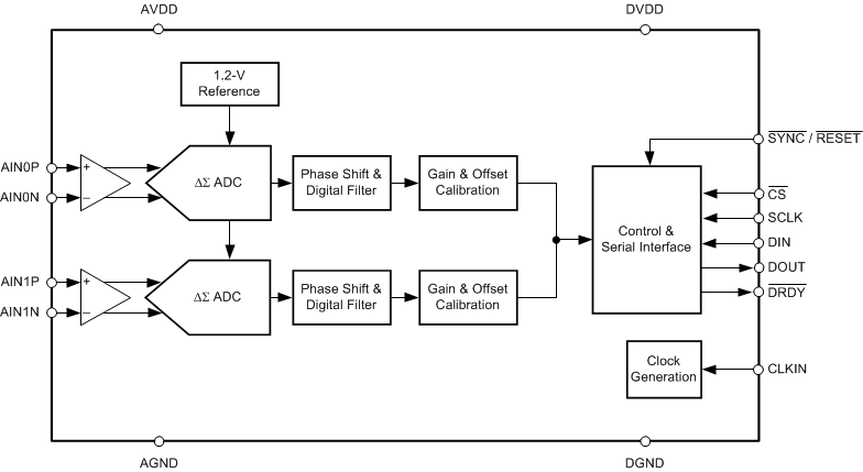
The ADS131M02-Q1 is a two-channel, simultaneously sampling, 24-bit, delta-sigma (ΔΣ), analog-to-digital converter (ADC) that offers wide dynamic range and low power, making the device designed for automotive battery management systems (BMS). The ADC inputs can be directly interfaced to shunt resistors for bidirectional battery-current measurements, to resistor-divider networks for high-voltage measurements, or to temperature sensors (such as thermistors or analog output temperature sensors).
The individual ADC channels can be independently configured depending on the sensor input. A low-noise, programmable gain amplifier (PGA) provides gains ranging from 1 to 128 to amplify low-level signals. Additionally, this device integrates channel-to-channel phase calibration and offset and gain calibration registers to help remove signal-chain errors.
A low-drift, 1.2-V reference is integrated into the device, reducing printed circuit board (PCB) area. Optional cyclic redundancy checks (CRCs) on the data input, data output, and register map maintain communication integrity.
The complete analog front-end (AFE) is offered in a 20-pin TSSOP package and is specified over the automotive temperature range of –40°C to +125°C.
| PART NUMBER | PACKAGE | BODY SIZE (NOM) |
|---|---|---|
| ADS131M02-Q1 | TSSOP (20) | 6.50 mm × 4.40 mm |
 Simplified Block Diagram