ZHCSOL7A March 2022 – August 2022 ADS131M04-Q1
PRODUCTION DATA
- 1 特性
- 2 应用
- 3 说明
- 4 Revision History
- 5 Pin Configuration and Functions
- 6 Specifications
- 7 Parameter Measurement Information
-
8 Detailed Description
- 8.1 Overview
- 8.2 Functional Block Diagram
- 8.3
Feature Description
- 8.3.1 Input ESD Protection Circuitry
- 8.3.2 Input Multiplexer
- 8.3.3 Programmable Gain Amplifier (PGA)
- 8.3.4 Voltage Reference
- 8.3.5 Clocking and Power Modes
- 8.3.6 ΔΣ Modulator
- 8.3.7 Digital Filter
- 8.3.8 DC Block Filter
- 8.3.9 Internal Test Signals
- 8.3.10 Channel Phase Calibration
- 8.3.11 Calibration Registers
- 8.3.12 Communication Cyclic Redundancy Check (CRC)
- 8.3.13 Register Map CRC
- 8.4 Device Functional Modes
- 8.5
Programming
- 8.5.1
Interface
- 8.5.1.1 Chip Select (CS)
- 8.5.1.2 Serial Data Clock (SCLK)
- 8.5.1.3 Serial Data Input (DIN)
- 8.5.1.4 Serial Data Output (DOUT)
- 8.5.1.5 Data Ready (DRDY)
- 8.5.1.6 Conversion Synchronization or System Reset (SYNC/RESET)
- 8.5.1.7 SPI Communication Frames
- 8.5.1.8 SPI Communication Words
- 8.5.1.9 ADC Conversion Data
- 8.5.1.10
Commands
- 8.5.1.10.1 NULL (0000 0000 0000 0000)
- 8.5.1.10.2 RESET (0000 0000 0001 0001)
- 8.5.1.10.3 STANDBY (0000 0000 0010 0010)
- 8.5.1.10.4 WAKEUP (0000 0000 0011 0011)
- 8.5.1.10.5 LOCK (0000 0101 0101 0101)
- 8.5.1.10.6 UNLOCK (0000 0110 0101 0101)
- 8.5.1.10.7 RREG (101a aaaa annn nnnn)
- 8.5.1.10.8 WREG (011a aaaa annn nnnn)
- 8.5.1.11 Short SPI Frames
- 8.5.2 Synchronization
- 8.5.1
Interface
- 8.6 ADS131M04-Q1 Registers
- 9 Application and Implementation
- 10Device and Documentation Support
- 11Mechanical, Packaging, and Orderable Information
8.5.1.9 ADC Conversion Data
The device provides conversion data for each channel at the data rate. The time when data are available relative to DRDY asserting is determined by the channel phase calibration setting and the DRDY_SEL[1:0] bits in the MODE register when in continuous-conversion mode. All data are available immediately following DRDY assertion in global-chop mode. The conversion status of all channels is available as the DRDY[3:0] bits in the STATUS register. The STATUS register content is automatically output as the response to the NULL command.
Conversion data are 24 bits. The data LSBs are truncated when the device operates with a 16-bit word size. The LSBs are zero padded or the MSBs sign extended when operating with a 32-bit word size depending on the setting of the WLENGTH[1:0] bits in the MODE register.
Data are given in binary two's complement format. Use Equation 10 to calculate the size of one code (LSB).
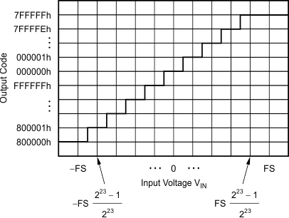
A positive full-scale input VIN ≥ +FSR – 1 LSB = 1.2 / Gain – 1 LSB produces an output code of 7FFFFFh and a negative full-scale input (VIN ≤ –FSR = –1.2 / Gain) produces an output code of 800000h. The output clips at these codes for signals that exceed full-scale.
Table 8-10 summarizes the ideal output codes for different input signals.
| INPUT SIGNAL, VIN = VAINP – VAINN |
IDEAL OUTPUT CODE |
|---|---|
| ≥ FSR (223 – 1) / 223 | 7FFFFFh |
| FSR / 223 | 000001h |
| 0 | 000000h |
| –FSR / 223 | FFFFFFh |
| ≤ –FSR | 800000h |
Figure 8-19 shows the mapping of the analog input signal to the output codes.
 Figure 8-19 Code Transition Diagram