ZHCSOP2 August 2022 ADS131M06-Q1
PRODUCTION DATA
- 1 特性
- 2 应用
- 3 说明
- 4 Revision History
- 5 Pin Configuration and Functions
- 6 Specifications
- 7 Parameter Measurement Information
-
8 Detailed Description
- 8.1 Overview
- 8.2 Functional Block Diagram
- 8.3
Feature Description
- 8.3.1 Input ESD Protection Circuitry
- 8.3.2 Input Multiplexer
- 8.3.3 Programmable Gain Amplifier (PGA)
- 8.3.4 Voltage Reference
- 8.3.5 Clocking and Power Modes
- 8.3.6 ΔΣ Modulator
- 8.3.7 Digital Filter
- 8.3.8 DC Block Filter
- 8.3.9 Internal Test Signals
- 8.3.10 Channel Phase Calibration
- 8.3.11 Calibration Registers
- 8.3.12 Communication Cyclic Redundancy Check (CRC)
- 8.3.13 Register Map CRC
- 8.4 Device Functional Modes
- 8.5
Programming
- 8.5.1
Interface
- 8.5.1.1 Chip Select (CS)
- 8.5.1.2 Serial Data Clock (SCLK)
- 8.5.1.3 Serial Data Input (DIN)
- 8.5.1.4 Serial Data Output (DOUT)
- 8.5.1.5 Data Ready (DRDY)
- 8.5.1.6 Conversion Synchronization or System Reset (SYNC/RESET)
- 8.5.1.7 SPI Communication Frames
- 8.5.1.8 SPI Communication Words
- 8.5.1.9 ADC Conversion Data
- 8.5.1.10
Commands
- 8.5.1.10.1 NULL (0000 0000 0000 0000)
- 8.5.1.10.2 RESET (0000 0000 0001 0001)
- 8.5.1.10.3 STANDBY (0000 0000 0010 0010)
- 8.5.1.10.4 WAKEUP (0000 0000 0011 0011)
- 8.5.1.10.5 LOCK (0000 0101 0101 0101)
- 8.5.1.10.6 UNLOCK (0000 0110 0101 0101)
- 8.5.1.10.7 RREG (101a aaaa annn nnnn)
- 8.5.1.10.8 WREG (011a aaaa annn nnnn)
- 8.5.1.11 Short SPI Frames
- 8.5.2 Synchronization
- 8.5.1
Interface
- 8.6 Registers
- 9 Application and Implementation
- 10Device and Documentation Support
- 11Mechanical, Packaging, and Orderable Information
8.4.6 Current-Detect Mode
Current-detect mode is a special mode that is helpful for applications requiring tamper detection when the equipment is in a low-power state. In this mode, the ADS131M06-Q1 collects a configurable number of samples at a nominal data rate of 2.7 kSPS and compares the absolute value of the results to a programmable threshold. If a configurable number of results exceed the threshold, the host is notified via a DRDY falling edge and the device returns to standby mode. Enter current-detect mode by providing a negative pulse on SYNC/RESET with a pulse duration less than tw(RSL) when in standby mode. Current-detect mode can only be entered from standby mode.
The device uses a limited power operating mode to generate conversions in current-detect mode. The conversion results are only used for comparison by the internal digital threshold comparator and are not accessible by the host. The device uses an internal oscillator that enables the device to capture the data without the use of the external clock input. Do not toggle CLKIN when in current-detect mode to minimize device power consumption. Do not place a capacitor on the REFIN pin if current-detect mode is used. Capacitance on this pin requires time to start up, and the resulting ADC conversions generated during current-detect mode are not valid when the voltage on the REFIN pin is charging.
Current-detect mode is configured in the CFG, THRSHLD_MSB, and THRSHLD_LSB registers. Enable and disable current-detect mode by toggling the CD_EN bit in the CFG register. The THRSHLD_MSB and THRSHLD_LSB registers contain the CD_THRSH[23:0] bits that represent the digital comparator threshold value during current detection.
The number of samples used for current detection are programmed by the CD_LEN[2:0] bits in the CFG register. The number of samples used for current detection range from 128 to 3584.
The programmable values in CD_NUM[2:0] configure the number of samples that must exceed the threshold for a detection to occur. The purpose of requiring multiple samples for detection is to control noisy values that may exceed the threshold, but do not represent a high enough power level to warrant action by the host. In summary, the conversion result must exceed the value programmed in CD_THRSH[23:0] a number of times as represented by the value stored in CD_NUM[2:0].
The device can be configured to notify the host based on any of the results from individual channels, all channels, or any combination of channels. The CD_ALLCH bit in the CFG register determines how many channels are required to exceed the programmed thresholds to trigger a current detection. When the bit is 1, all enabled channels are required to meet the current detection requirements in order for the host to be notified. If the bit is 0, any enabled channel triggers a current detection notification if the requirements are met. Enable and disable channels using the CHn_EN bits in the CLK register to control which combination of channels must meet the requirements to trigger a current-detection notification.
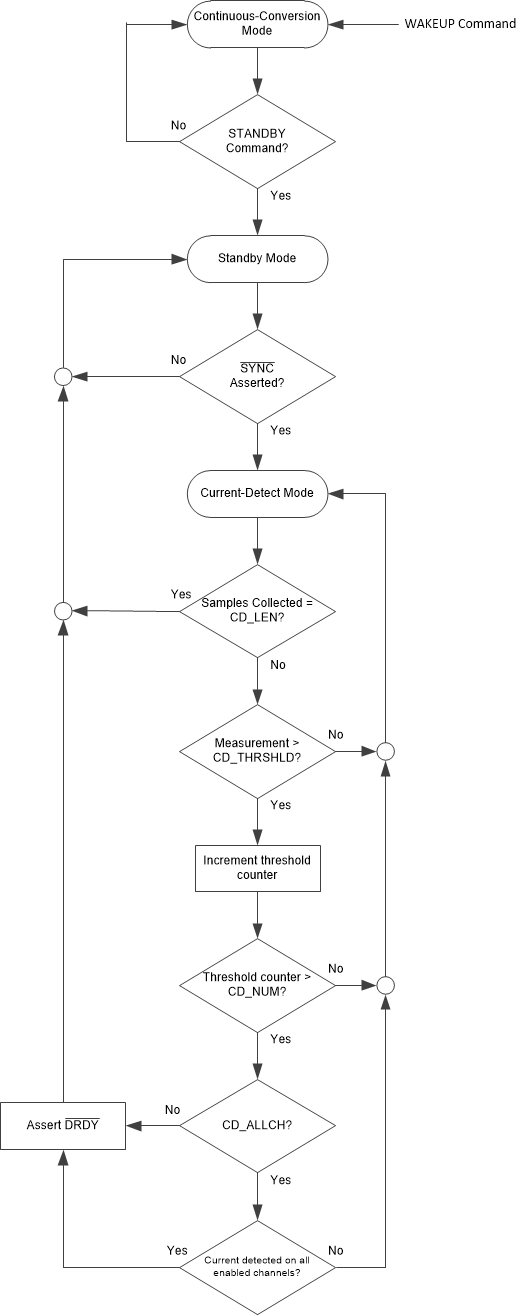
Figure 8-17 illustrates a flow chart depicting the current-detection process on the ADS131M06-Q1.
 Figure 8-17 Current-Detect Mode Flow Chart