ZHCS054C February 2011 – June 2017 ADS4122 , ADS4125 , ADS4142 , ADS4145
PRODUCTION DATA.
- 1 特性
- 2 应用
- 3 说明
- 4 修订历史记录
- 5 Device Family Comparison
- 6 Pin Configuration and Functions
-
7 Specifications
- 7.1 Absolute Maximum Ratings
- 7.2 ESD Ratings
- 7.3 Recommended Operating Conditions
- 7.4 Thermal Information
- 7.5 Electrical Characteristics: ADS412x
- 7.6 Electrical Characteristics: ADS414x
- 7.7 Electrical Characteristics: General
- 7.8 Digital Characteristics
- 7.9 Timing Requirements: LVDS and CMOS Modes
- 7.10 Serial Interface Timing Characteristics
- 7.11 Reset Timing Requirements
- 7.12 Timing Characteristics at Lower Sampling Frequencies
- 7.13 Typical Characteristics: ADS4122
- 7.14 Typical Characteristics: ADS4125
- 7.15 Typical Characteristics: ADS4142
- 7.16 Typical Characteristics: ADS4145
- 7.17 Typical Characteristics: Common
- 7.18 Typical Characteristics: Contour
- 8 Detailed Description
- 9 Application and Implementation
- 10Power Supply Recommendations
- 11Layout
- 12器件和文档支持
- 13机械、封装和可订购信息
8 Detailed Description
8.1 Overview
The ADS412x and ADS414x devices are high-performance, low-power, 12-bit and 14-bit analog-to-digital converters (ADCs) with maximum sampling rates up to 65 MSPS and 125 MSPS. The conversion process is initiated by a rising edge of the external input clock when the analog input signal is sampled. The sampled signal is sequentially converted by a series of small resolution stages, with the outputs combined in a digital correction logic block. At every clock edge, the sample propagates through the pipeline, resulting in a data latency of 10 clock cycles. The output is available as 12-bit and 14-bit data, in DDR LVDS mode or CMOS mode, and coded in either straight offset binary or binary twos complement format.
The ADS412x and ADS414x family is pin-compatible to the previous generation ADS6149 family; this architecture enables easy migration. However, there are some important differences between the generations, summarized in Table 1.
Table 1. Migrating from the ADS6149 Family
| ADS6149 FAMILY | ADS4145 FAMILY |
|---|---|
| PINS | |
| Pin 21 is NC (not connected) | Pin 21 is NC (not connected) |
| Pin 23 is MODE | Pin 23 is RESERVED in the ADS4145 family. It is reserved as a digital control pin for an (as yet) undefined function in the next-generation ADC series. |
| SUPPLY | |
| AVDD is 3.3 V | AVDD is 1.8 V |
| DRVDD is 1.8 V | No change |
| INPUT COMMON-MODE VOLTAGE | |
| VCM is 1.5 V | VCM is 0.95 V |
| SERIAL INTERFACE | |
| Protocol: 8-bit register address and 8-bit register data | No change in protocol |
| New serial register map | |
| EXTERNAL REFERENCE MODE | |
| Supported | Not supported |
| ADS61B49 FAMILY | ADS41B29, ADS41B49, ADS58B18 FAMILY |
| PINS | |
| Pin 21 is NC (not connected) | Pin 21 is 3.3 V AVDD_BUF (supply for the analog input buffers) |
| Pin 23 is MODE | Pin 23 is a digital control pin for the RESERVED function. Pin 23 functions as SNR Boost enable (B18 only). |
| SUPPLY | |
| AVDD is 3.3 V | AVDD is 1.8 V, AVDD_BUF is 3.3 V |
| DRVDD is 1.8 V | No change |
| INPUT COMMON-MODE VOLTAGE | |
| VCM is 1.5 V | VCM is 1.7 V |
| SERIAL INTERFACE | |
| Protocol: 8-bit register address and 8-bit register data | No change in protocol New serial register map |
| EXTERNAL REFERENCE MODE | |
| Supported | Not supported |
8.2 Functional Block Diagrams
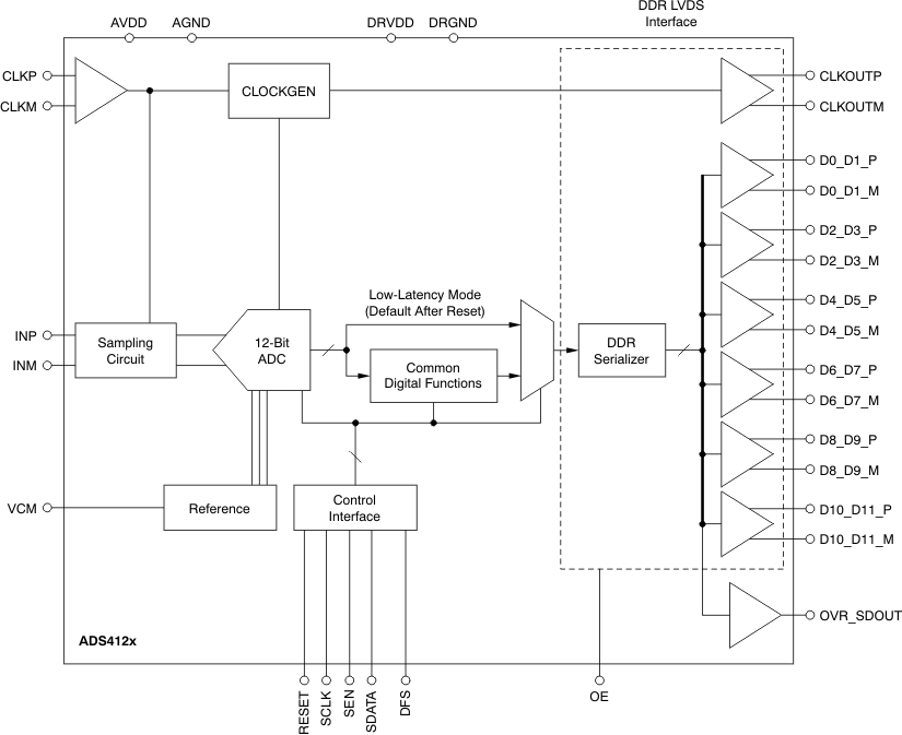 Figure 93. ADS412x Block Diagram
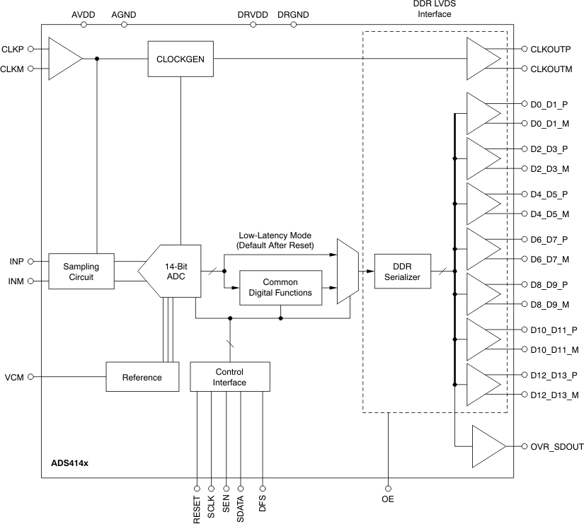 Figure 94. ADS414x Block Diagram
8.3 Feature Description
8.3.1 Digital Functions and Low-Latency Mode
The device has several useful digital functions such as test patterns, gain, and offset correction. All of these functions require extra clock cycles for operation and increase the overall latency and power of the device. Alternately, the device has a low-latency mode in which the raw ADC output is routed to the output data pins with a latency of 10 clock cycles. In this mode, the digital functions are bypassed. Figure 95 shows more details of the processing after the ADC.
The device is in low-latency mode after reset. In order to use any of the digital functions, the low-latency mode must first be disabled by setting the DIS LOW LATENCY register bit to 1. After this process, the respective register bits must be programmed as described in the following sections and in the Serial Register Map section.
 Figure 95. Digital Processing Block Diagram
8.3.2 Gain for SFDR, SNR Trade-Off
The ADS412x and ADS414x include gain settings that can be used to improve SFDR performance. The gain is programmable from 0 dB to 6 dB (in 0.5-dB steps) using the GAIN register bits. For each gain setting, the analog input full-scale range scales proportionally, as shown in Table 2.
The SFDR improvement is achieved at the expense of SNR; for each gain setting, the SNR degrades approximately between 0.5 dB and 1 dB. The SNR degradation is reduced at high input frequencies. As a result, the gain is very useful at high input frequencies because the SFDR improvement is significant with marginal degradation in SNR. Therefore, the gain can be used to trade-off between SFDR and SNR.
After a reset, the device is in low-latency mode and gain function is disabled. To use gain:
- First, disable the low-latency mode (DIS LOW LATENCY = 1).
- This setting enables the gain and puts the device in a 0-dB gain mode.
- For other gain settings, program the GAIN bits.
Table 2. Full-Scale Range Across Gains
| GAIN (dB) | TYPE | FULL-SCALE (VPP) |
|---|---|---|
| 0 | Default after reset | 2 |
| 1 | Programmable | 1.78 |
| 2 | Programmable | 1.59 |
| 3 | Programmable | 1.42 |
| 4 | Programmable | 1.26 |
| 5 | Programmable | 1.12 |
| 6 | Programmable | 1 |
8.3.3 Offset Correction
The ADS412x and ADS414x have an internal offset correction algorithm that estimates and corrects dc offset up to ±10 mV. The correction can be enabled using the EN OFFSET CORR serial register bit. When enabled, the algorithm estimates the channel offset and applies the correction every clock cycle. The time constant of the correction loop is a function of the sampling clock frequency. The time constant can be controlled using the OFFSET CORR TIME CONSTANT register bits, as described in Table 3.
Table 3. Time Constant of Offset Correction Loop
| OFFSET CORR TIME CONSTANT | TIME CONSTANT, TCCLK
(Number of Clock Cycles) |
TIME CONSTANT, TCCLK × 1/fS (sec)(1) |
|---|---|---|
| 0000 | 1M | 8 ms |
| 0001 | 2M | 16 ms |
| 0010 | 4M | 33.4 ms |
| 0011 | 8M | 67 ms |
| 0100 | 16M | 134 ms |
| 0101 | 32M | 268 ms |
| 0110 | 64M | 537 ms |
| 0111 | 128M | 1.08 s |
| 1000 | 256M | 2.15 s |
| 1001 | 512M | 4.3 s |
| 1010 | 1G | 8.6 s |
| 1011 | 2G | 17.2 s |
| 1100 | Reserved | — |
| 1101 | Reserved | — |
| 1110 | Reserved | — |
| 1111 | Reserved | — |
After the offset is estimated, the correction can be frozen by setting FREEZE OFFSET CORR = 1. When frozen, the last estimated value is used for the offset correction of every clock cycle. Note that offset correction is disabled by a default after reset.
After a reset, the device is in low-latency mode and offset correction is disabled. To use offset correction:
- First, disable the low-latency mode (DIS LOW LATENCY = 1).
- Then set EN OFFSET CORR to 1 and program the required time constant.
Figure 96 shows the time response of the offset correction algorithm after being enabled.
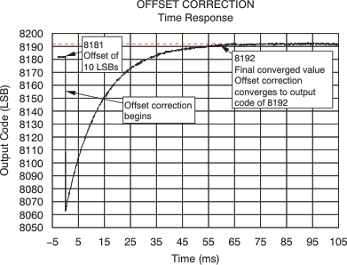 Figure 96. Time Response of Offset Correction
8.3.4 Power-Down
The ADS412x and ADS414x have three power-down modes: power-down global, standby, and output buffer disable.
8.3.4.1 Power-Down Global
In this mode, the entire device (including the ADC, internal reference, and the output buffers) is powered down, resulting in reduced total power dissipation of approximately 10 mW. The output buffers are in a high-impedance state. The wake-up time from the global power-down to data becoming valid in normal mode is typically 100 µs. To enter the global power-down mode, set the PDN GLOBAL register bit.
8.3.4.2 Standby
In this mode, only the ADC is powered down and the internal references are active, resulting in a fast wake-up time of 5 µs. The total power dissipation in standby mode is approximately 130 mW at 125 MSPS. To enter the standby mode, set the STBY register bit.
8.3.4.3 Output Buffer Disable
The output buffers can be disabled and put in a high-impedance state; wake-up time from this mode is fast, approximately 100 ns. Disabling the output buffers can be controlled using the PDN OBUF register bit or using the OE pin.
8.3.4.4 Input Clock Stop
In addition, the converter enters a low-power mode when the input clock frequency falls below 1 MSPS. The power dissipation is approximately 80 mW.
8.3.5 Output Data Format
Two output data formats are supported: twos complement and offset binary. Each mode can be selected using the DATA FORMAT serial interface register bit or controlling the DFS pin in parallel configuration mode. In the event of an input voltage overdrive, the digital outputs go to the appropriate full-scale level.
8.4 Device Functional Modes
8.4.1 Digital Output Information
The ADS412x and ADS414x provide either 14-bit data or 12-bit data, respectively, and an output clock synchronized with the data.
8.4.1.1 Output Interface
Two output interface options are available: double data rate (DDR) LVDS and parallel CMOS. These options can be selected using the LVDS CMOS serial interface register bit or using the DFS pin.
8.4.1.2 DDR LVDS Outputs
In this mode, the data bits and clock are output using low voltage differential signal (LVDS) levels. Two data bits are multiplexed and output on each LVDS differential pair, as shown in Figure 97 and Figure 98.
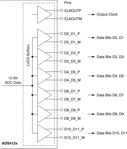 Figure 97. ADS412x LVDS Data Outputs
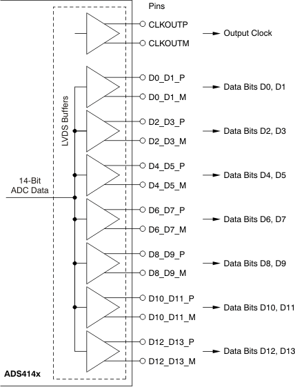 Figure 98. ADS414x LVDS Data Outputs
Even data bits (D0, D2, D4, and so forth) are output at the falling edge of CLKOUTP and the odd data bits (D1, D3, D5, and so forth) are output at the rising edge of CLKOUTP. Both the rising and falling edges of CLKOUTP must be used to capture all 14 data bits, as shown in Figure 99.
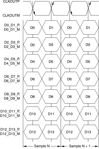 Figure 99. DDR LVDS Interface
8.4.1.3 LVDS Output Data and Clock Buffers
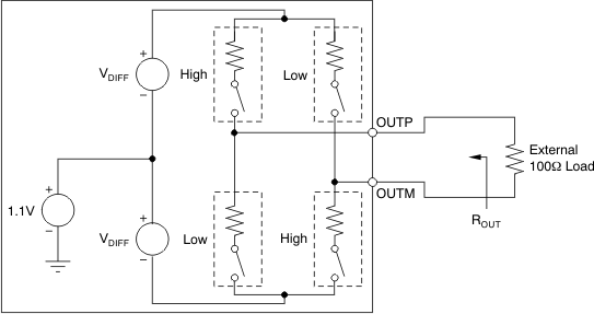
The equivalent circuit of each LVDS output buffer is shown in Figure 100. After reset, the buffer presents an output impedance of 100 Ω to match with the external 100-Ω termination.
The VDIFF voltage is nominally 350 mV, resulting in an output swing of ±350 mV with 100-Ω external termination. The VDIFF voltage is programmable using the LVDS SWING register bits from ±125 mV to ±570 mV.
Additionally, a mode exists to double the strength of the LVDS buffer to support 50-Ω differential termination. This mode can be used when the output LVDS signal is routed to two separate receiver chips, each using a 100-Ω termination. The mode can be enabled using the LVDS DATA STRENGTH and LVDS CLKOUT STRENGTH register bits for data and output clock buffers, respectively.
The buffer output impedance behaves in the same way as a source-side series termination. By absorbing reflections from the receiver end, the output impedance of buffer helps improve signal integrity.
8.4.1.4 Parallel CMOS Interface
In CMOS mode, each data bit is output on a separate pin as the CMOS voltage level, for every clock cycle. The rising edge of the output clock CLKOUT can be used to latch data in the receiver. Figure 101 depicts the CMOS output interface.
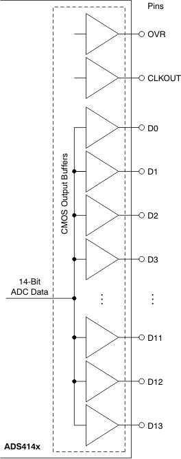 Figure 101. CMOS Output Interface
Switching noise (caused by CMOS output data transitions) can couple into the analog inputs and degrade SNR. The coupling and SNR degradation increases as the output buffer drive is made stronger. To minimize this degradation, the CMOS output buffers are designed with controlled drive strength. The default drive strength ensures a wide data stable window. TI recommends using short traces (one to two inches or 2.54 cm to 5.08 cm) terminated with less than 5-pF load capacitance, as shown in Figure 102.
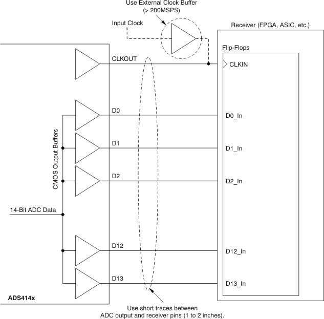 Figure 102. Using the CMOS Data Outputs
8.4.1.5 CMOS Interface Power Dissipation
With CMOS outputs, the DRVDD current scales with the sampling frequency and the load capacitance on every output pin. The maximum DRVDD current occurs when each output bit toggles between 0 and 1 every clock cycle. In actual applications, this condition is unlikely to occur. The actual DRVDD current is determined by the average number of output bits switching, which is a function of the sampling frequency and the nature of the analog input signal.
where
Figure 86 details the current across sampling frequencies at 2-MHz analog input frequency.
8.5 Programming
The performance of the ADS41xx can be enhanced by writing certain SPI registers bits with minimal impact (less than 10 mW) on power consumption. Table 4 lists the device high-performance modes.
Table 4. High-Performance Modes(1)(2)(3)
| PARAMETER | DESCRIPTION |
|---|---|
| Mode 1 | Set the MODE 1 register bits to get best performance across sample clock and input signal frequencies. Register address = 03h, register data = 03h |
| Mode 2 | Set the MODE 2 register bit to get best performance at high input signal frequencies greater than 230 MHz. Register address = 4Ah, register data = 01h |
8.5.1 Device Configuration
The ADS412x and ADS414x have several modes that can be configured using a serial programming interface, as described in Table 5, Table 6, and Table 7. In addition, the devices have two dedicated parallel pins for quickly configuring commonly used functions. The parallel pins are DFS (analog 4-level control pin) and OE (digital control pin). The analog control pins can be easily configured using a simple resistor divider (with 10% tolerance resistors).
Table 5. DFS: Analog Control Pin
| VOLTAGE APPLIED ON DFS | DESCRIPTION (Data Format, Output Interface) |
|---|---|
| 0, 100 mV, –0 mV | Twos complement, DDR LVDS |
| (3/8) AVDD ± 100 mV | Twos complement, parallel CMOS |
| (5/8) AVDD ± 100 mV | Offset binary, parallel CMOS |
| AVDD, 0 mV, –100 mV | Offset binary, DDR LVDS |
Table 6. OE: Digital Control Pin
| VOLTAGE APPLIED ON OE | DESCRIPTION |
|---|---|
| 0 | Output data buffers disabled |
| AVDD | Output data buffers enabled |
When the serial interface is not used, the SDATA pin can also be used as a digital control pin to place the device in standby mode. To enable this functionality, the RESET pin must be tied high. In this mode, SEN and SCLK do not have any alternative functions. Keep SEN tied high and SCLK tied low on the board.
Table 7. SDATA: Digital Control Pin
| VOLTAGE APPLIED ON SDATA | DESCRIPTION |
|---|---|
| 0 | Normal operation |
| Logic high | Device enters standby |
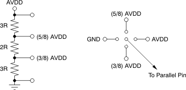 Figure 103. Simplified Diagram to Configure the DFS Pin
8.5.2 Serial Interface
The analog-to-digital converter (ADC) has a set of internal registers that can be accessed by the serial interface formed by the SEN (serial interface enable), SCLK (serial interface clock), and SDATA (serial interface data) pins. Serially shifting bits into the device is enabled when SEN is low. Serial data SDATA are latched at every falling edge of SCLK when SEN is active (low). The serial data are loaded into the register at every 16th SCLK falling edge when SEN is low. If the word length exceeds a multiple of 16 bits, the excess bits are ignored. Data can be loaded in multiples of 16-bit words within a single active SEN pulse. The first eight bits form the register address and the remaining eight bits are the register data. The interface can work with SCLK frequency from 20 MHz down to very low speeds (a few hertz) and also with a non-50% SCLK duty cycle.
8.5.2.1 Register Initialization
After power-up, the internal registers must be initialized to the default values. This initialization can be accomplished in one of two ways:
- Either through hardware reset by applying a high pulse on RESET pin (of durations greater than 10 ns), as shown in Figure 5; or
- By applying a software reset. When using the serial interface, set the RESET bit (D7 in register 00h) high. This setting initializes the internal registers to the default values and then self-resets the RESET bit low. In this case, the RESET pin is kept low.
8.5.3 Serial Register Readout
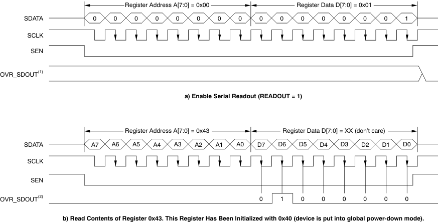
The serial register readout function allows the contents of the internal registers to be read back on the OVR_SDOUT pin. This readback may be useful as a diagnostic check to verify the serial interface communication between the external controller and the ADC.
After power-up and device reset, the OVR_SDOUT pin functions as an over-range indicator pin by default. When the readout mode is enabled, OVR_SDOUT outputs the contents of the selected register serially:
- Set the READOUT register bit to 1. This setting puts the device in serial readout mode and disables any further writes to the internal registers except the register at address 0. Note that the READOUT bit itself is also located in register 0. The device can exit readout mode by writing READOUT = 0. Only the contents of the register at address 0 cannot be read in the register readout mode.
- Initiate a serial interface cycle specifying the address of the register (A7 to A0) whose content must be read.
- The device serially outputs the contents (D7 to D0) of the selected register on the OVR_SDOUT pin.
- The external controller can latch the contents at the falling edge of SCLK.
- To exit the serial readout mode, the reset register bit READOUT = 0 enables writes into all registers of the device. At this point, the OVR_SDOUT pin becomes an over-range indicator pin.
8.6 Register Maps
8.6.1 Serial Register Map
Table 8 summarizes the functions supported by the serial interface.
Table 8. Serial Interface Register Map(1)
| REGISTER ADDRESS | DEFAULT VALUE AFTER RESET | REGISTER DATA | |||||||
|---|---|---|---|---|---|---|---|---|---|
| A[7:0] (Hex) | D[7:0] (Hex) | D7 | D6 | D5 | D4 | D3 | D2 | D1 | D0 |
| 00 | 00 | 0 | 0 | 0 | 0 | 0 | 0 | RESET | READOUT |
| 01 | 00 | LVDS SWING | 0 | 0 | |||||
| 03 | 00 | 0 | 0 | 0 | 0 | 0 | 0 | HIGH PERF MODE 1 | |
| 25 | 00 | GAIN | DISABLE GAIN | TEST PATTERNS | |||||
| 26 | 00 | 0 | 0 | 0 | 0 | 0 | 0 | LVDS CLKOUT STRENGTH | LVDS DATA STRENGTH |
| 3D | 00 | DATA FORMAT | EN OFFSET CORR | 0 | 0 | 0 | 0 | 0 | |
| 3F | 00 | CUSTOM PATTERN HIGH D[13:6] | |||||||
| 40 | 00 | CUSTOM PATTERN D[5:0] | 0 | 0 | |||||
| 41 | 00 | LVDS CMOS | CMOS CLKOUT STRENGTH | EN CLKOUT RISE | CLKOUT RISE POSN | EN CLKOUT FALL | |||
| 42 | 00 | CLKOUT FALL POSN | 0 | 0 | DIS LOW LATENCY | STBY | 0 | 0 | |
| 43 | 00 | 0 | PDN GLOBAL | 0 | PDN OBUF | 0 | 0 | EN LVDS SWING | |
| 4A | 00 | 0 | 0 | 0 | 0 | 0 | 0 | 0 | HIGH PERF MODE 2 |
| BF | 00 | OFFSET PEDESTAL | 0 | 0 | |||||
| CF | 00 | FREEZE OFFSET CORR | 0 | OFFSET CORR TIME CONSTANT | 0 | 0 | |||
| DF | 00 | 0 | 0 | LOW SPEED | 0 | 0 | 0 | 0 | |
8.6.2 Description of Serial Registers
For best performance, two special mode register bits must be enabled: HI PERF MODE 1 and HI PERF MODE 2.
Table 1. Register Address 00h (Default = 00h)
| 7 | 6 | 5 | 4 | 3 | 2 | 1 | 0 |
| 0 | 0 | 0 | 0 | 0 | 0 | RESET | READOUT |
| Bits[7:2] | Always write 0 |
| Bit 1 | RESET: Software reset applied |
| This bit resets all internal registers to the default values and self-clears to 0 (default = 1). | |
| Bit 0 | READOUT: Serial readout |
| This bit sets the serial readout of the registers. 0 = Serial readout of registers disabled; the OVR_SDOUT pin functions as an overvoltage indicator. 1 = Serial readout enabled; the OVR_SDOUT pin functions as a serial data readout. |
Table 2. Register Address 01h (Default = 00h)
| 7 | 6 | 5 | 4 | 3 | 2 | 1 | 0 |
| LVDS SWING | 0 | 0 | |||||
| Bits[7:2] | LVDS SWING: LVDS swing programmability(1) |
| 000000 = Default LVDS swing; ±350 mV with external 100-Ω termination 011011 = LVDS swing increases to ±410 mV 110010 = LVDS swing increases to ±465 mV 010100 = LVDS swing increases to ±570 mV 111110 = LVDS swing decreases to ±200 mV 001111 = LVDS swing decreases to ±125 mV |
|
| Bits[1:0] | Always write 0 |
Table 3. Register Address 03h (Default = 00h)
| 7 | 6 | 5 | 4 | 3 | 2 | 1 | 0 |
| 0 | 0 | 0 | 0 | 0 | 0 | HI PERF MODE 1 | |
| Bits[7:2] | Always write 0 |
| Bits[1:0] | HI PERF MODE 1: High performance mode 1 |
| 00 = Default performance after reset 01 = Do not use 10 = Do not use 11 = For best performance across sampling clock and input signal frequencies, set the HIGH PERF MODE 1 bits |
Table 4. Register Address 25h (Default = 00h)
| 7 | 6 | 5 | 4 | 3 | 2 | 1 | 0 |
| GAIN | DISABLE GAIN | TEST PATTERNS | |||||
| Bits[7:4] | GAIN: Gain programmability | ||
| These bits set the gain programmability in 0.5-dB steps. | |||
| 0000 = 0-dB gain (default after reset) 0001 = 0.5-dB gain 0010 = 1.0-dB gain 0011 = 1.5-dB gain 0100 = 2.0-dB gain 0101 = 2.5-dB gain 0110 = 3.0-dB gain |
0111 = 3.5-dB gain 1000 = 4.0-dB gain 1001 = 4.5-dB gain 1010 = 5.0-dB gain 1011 = 5.5-dB gain 1100 = 6-dB gain |
||
| Bit 3 | DISABLE GAIN: Gain setting | ||
| This bit sets the gain. 0 = Gain enabled; gain is set by the GAIN bits only if low-latency mode is disabled 1 = Gain disabled |
|||
| Bits[2:0] | TEST PATTERNS: Data capture | ||
| These bits verify data capture. 000 = Normal operation 001 = Outputs all 0s 010 = Outputs all 1s 011 = Outputs toggle pattern |
|||
| In the ADS4122/25, output data D[11:0] is an alternating sequence of 010101010101 and 101010101010. In the ADS4142/45, output data D[13:0] is an alternating sequence of 01010101010101 and 10101010101010. |
|||
| 100 = Outputs digital ramp | |||
| In ADS4122/25, output data increments by one LSB (12-bit) every fourth clock cycle from code 0 to code 4095 In ADS4142/45, output data increments by one LSB (14-bit) every clock cycle from code 0 to code 16383 |
|||
| 101 = Output custom pattern (use registers 3Fh and 40h for setting the custom pattern) 110 = Unused 111 = Unused |
|||
Table 5. Register Address 26h (Default = 00h)
| 7 | 6 | 5 | 4 | 3 | 2 | 1 | 0 |
| 0 | 0 | 0 | 0 | 0 | 0 | LVDS CLKOUT STRENGTH | LVDS DATA STRENGTH |
| Bits[7:2] | Always write 0 |
| Bit 1 | LVDS CLKOUT STRENGTH: LVDS output clock buffer strength |
| This bit determines the external termination to be used with the LVDS output clock buffer. 0 = 100-Ω external termination (default strength) 1 = 50-Ω external termination (2x strength) |
|
| Bit 0 | LVDS DATA STRENGTH: LVDS data buffer strength |
| This bit determines the external termination to be used with all of the LVDS data buffers. 0 = 100-Ω external termination (default strength) 1 = 50-Ω external termination (2x strength) |
Table 6. Register Address 3Dh (Default = 00h)
| 7 | 6 | 5 | 4 | 3 | 2 | 1 | 0 |
| DATA FORMAT | EN OFFSET CORR | 0 | 0 | 0 | 0 | 0 | |
| Bits[7:6] | DATA FORMAT: Data format selection |
| These bits selects the data format. 00 = The DFS pin controls data format selection 10 = Twos complement 11 = Offset binary |
|
| Bit 5 | ENABLE OFFSET CORR: Offset correction setting |
| This bit sets the offset correction. 0 = Offset correction disabled 1 = Offset correction enabled |
|
| Bits[4:0] | Always write 0 |
Table 7. Register Address 3Fh (Default = 00h)
| 7 | 6 | 5 | 4 | 3 | 2 | 1 | 0 |
| CUSTOM PATTERN D13 | CUSTOM PATTERN D12 | CUSTOM PATTERN D11 | CUSTOM PATTERN D10 | CUSTOM PATTERN D9 | CUSTOM PATTERN D8 | CUSTOM PATTERN D7 | CUSTOM PATTERN D6 |
| Bits[7:0] | CUSTOM PATTERN(1) |
| These bits set the custom pattern. |
Table 8. Register Address 40h (Default = 00h)
| 7 | 6 | 5 | 4 | 3 | 2 | 1 | 0 |
| CUSTOM PATTERN D5 | CUSTOM PATTERN D4 | CUSTOM PATTERN D3 | CUSTOM PATTERN D2 | CUSTOM PATTERN D1 | CUSTOM PATTERN D0 | 0 | 0 |
| Bits[7:2] | CUSTOM PATTERN(1) |
| These bits set the custom pattern. | |
| Bits[1:0] | Always write 0 |
Table 9. Register Address 41h (Default = 00h)
| 7 | 6 | 5 | 4 | 3 | 2 | 1 | 0 |
| LVDS CMOS | CMOS CLKOUT STRENGTH | EN CLKOUT RISE | CLKOUT RISE POSN | EN CLKOUT FALL | |||
| Bits[7:6] | LVDS CMOS: Interface selection |
| These bits select the interface. 00 = The DFS pin controls the selection of either LVDS or CMOS interface 10 = The DFS pin controls the selection of either LVDS or CMOS interface 01 = DDR LVDS interface 11 = Parallel CMOS interface |
|
| Bits[5:4] | CMOS CLKOUT STRENGTH |
| Controls strength of CMOS output clock only. 00 = Maximum strength (recommended and used for specified timings) 01 = Medium strength 10 = Low strength 11 = Very low strength |
|
| Bit 3 | ENABLE CLKOUT RISE |
| 0 = Disables control of output clock rising edge 1 = Enables control of output clock rising edge |
|
| Bits[2:1] | CLKOUT RISE POSN: CLKOUT rise control |
| Controls position of output clock rising edge | |
| LVDS interface: 00 = Default position (timings are specified in this condition) 01 = Setup reduces by 500 ps, hold increases by 500 ps 10 = Data transition is aligned with rising edge 11 = Setup reduces by 200 ps, hold increases by 200 ps |
|
| CMOS interface: 00 = Default position (timings are specified in this condition) 01 = Setup reduces by 100 ps, hold increases by 100 ps 10 = Setup reduces by 200 ps, hold increases by 200 ps 11 = Setup reduces by 1.5 ns, hold increases by 1.5 ns |
|
| Bit 0 | ENABLE CLKOUT FALL |
| 0 = Disables control of output clock fall edge 1 = Enables control of output clock fall edge |
Table 10. Register Address 42h (Default = 00h)
| 7 | 6 | 5 | 4 | 3 | 2 | 1 | 0 |
| CLKOUT FALL CTRL | 0 | 0 | DIS LOW LATENCY | STBY | 0 | 0 | |
| Bits[7:6] | CLKOUT FALL CTRL |
| Controls position of output clock falling edge | |
| LVDS interface: 00 = Default position (timings are specified in this condition) 01 = Setup reduces by 400 ps, hold increases by 400 ps 10 = Data transition is aligned with rising edge 11 = Setup reduces by 200 ps, hold increases by 200 ps |
|
| CMOS interface: 00 = Default position (timings are specified in this condition) 01 = Falling edge is advanced by 100 ps 10 = Falling edge is advanced by 200 ps 11 = Falling edge is advanced by 1.5 ns |
|
| Bits[5:4] | Always write 0 |
| Bit 3 | DIS LOW LATENCY: Disable low latency |
| This bit disables low-latency mode, 0 = Low-latency mode is enabled. Digital functions such as gain, test patterns and offset correction are disabled 1 = Low-latency mode is disabled. This setting enables the digital functions. See the Digital Functions and Low Latency Mode section. |
|
| Bit 2 | STBY: Standby mode |
| This bit sets the standby mode. 0 = Normal operation 1 = Only the ADC and output buffers are powered down; internal reference is active; wake-up time from standby is fast |
|
| Bits[1:0] | Always write 0 |
Table 11. Register Address 43h (Default = 00h)
| 7 | 6 | 5 | 4 | 3 | 2 | 1 | 0 |
| 0 | PDN GLOBAL | 0 | PDN OBUF | 0 | 0 | EN LVDS SWING | |
| Bit 0 | Always write 0 |
| Bit 6 | PDN GLOBAL: Power-down |
| This bit sets the state of operation. 0 = Normal operation 1 = Total power down; the ADC, internal references, and output buffers are powered down; slow wake-up time. |
|
| Bit 5 | Always write 0 |
| Bit 4 | PDN OBUF: Power-down output buffer |
| This bit set the output data and clock pins. 0 = Output data and clock pins enabled 1 = Output data and clock pins powered down and put in high- impedance state |
|
| Bits[3:2] | Always write 0 |
| Bits[1:0] | EN LVDS SWING: LVDS swing control |
| 00 = LVDS swing control using LVDS SWING register bits is disabled 01 = Do not use 10 = Do not use 11 = LVDS swing control using LVDS SWING register bits is enabled |
Table 12. Register Address 4Ah (Default = 00h)
| 7 | 6 | 5 | 4 | 3 | 2 | 1 | 0 |
| 0 | 0 | 0 | 0 | 0 | 0 | 0 | HI PERF MODE 2 |
| Bits[7:1] | Always write 0 |
| Bit[0] | HI PERF MODE 2: High performance mode 2 |
| This bit is recommended for high input signal frequencies greater than 230 MHz. 0 = Default performance after reset 1 = For best performance with high-frequency input signals, set the HIGH PERF MODE 2 bit |
Table 13. Register Address BFh (Default = 00h)
| 7 | 6 | 5 | 4 | 3 | 2 | 1 | 0 |
| OFFSET PEDESTAL | 0 | 0 | |||||
| Bits[7:2] | OFFSET PEDESTAL | |
| These bits set the offset pedestal. When the offset correction is enabled, the final converged value after the offset is corrected is the ADC mid-code value. A pedestal can be added to the final converged value by programming these bits. |
||
| ADS414x VALUE | PEDESTAL | |
| 011111 011110 011101 — 000000 — 111111 111110 — 100000 |
31 LSB 30 LSB 29 LSB — 0 LSB — –1 LSB –2 LSB — –32 LSB |
|
| Bits[1:0] | Always write 0 | |
Table 14. Register Address CFh (Default = 00h)
| 7 | 6 | 5 | 4 | 3 | 2 | 1 | 0 |
| FREEZE OFFSET CORR | 0 | OFFSET CORR TIME CONSTANT | 0 | 0 | |||
| Bit 7 | FREEZE OFFSET CORR | |
| This bit sets the freeze offset correction. 0 = Estimation of offset correction is not frozen (bit EN OFFSET CORR must be set) 1 = Estimation of offset correction is frozen (bit EN OFFSET CORR must be set). When frozen, the last estimated value is used for offset correction every clock cycle. See the Offset Correction section. |
||
| Bit 6 | Always write 0 | |
| Bits[5:2] | OFFSET CORR TIME CONSTANT | |
| These bits set the offset correction time constant for the correction loop time constant in number of clock cycles. | ||
| VALUE | TIME CONSTANT (Number of Clock Cycles) | |
| 0000 0001 0010 0011 0100 0101 0110 0111 1000 1001 1010 1011 |
1M 2M 4M 8M 16M 32M 64M 128M 256M 512M 1G 2G |
|
| Bits[1:0] | Always write 0 | |
Table 15. Register Address DFh (Default = 00h)
| 7 | 6 | 5 | 4 | 3 | 2 | 1 | 0 |
| 0 | 0 | LOW SPEED | 0 | 0 | 0 | 0 | |
| Bits[7:6] | Always write 0 | |
| Bits[5:4] | LOW SPEED: Low-speed mode | |
| For the ADS4122/42, the low-speed mode is enabled by default after reset. 00, 01, 10, 11 = Do not use |
||
| For the ADS4125/55 only: 00, 01, 10 = Low-speed mode disabled (default state after reset); this setting is recommended for sampling rates greater than 80 MSPS. 11 = Low-speed mode enabled; this setting is recommended for sampling rates less than or equal to 80 MSPS. |
||
| Bits[3:0] | Always write 0 | |