ZHCS054C February   2011  – June 2017 ADS4122 , ADS4125 , ADS4142 , ADS4145

PRODUCTION DATA.  

  1. 特性
  2. 应用
  3. 说明
  4. 修订历史记录
  5. Device Family Comparison
  6. Pin Configuration and Functions
  7. Specifications
    1. 7.1  Absolute Maximum Ratings
    2. 7.2  ESD Ratings
    3. 7.3  Recommended Operating Conditions
    4. 7.4  Thermal Information
    5. 7.5  Electrical Characteristics: ADS412x
    6. 7.6  Electrical Characteristics: ADS414x
    7. 7.7  Electrical Characteristics: General
    8. 7.8  Digital Characteristics
    9. 7.9  Timing Requirements: LVDS and CMOS Modes
    10. 7.10 Serial Interface Timing Characteristics
    11. 7.11 Reset Timing Requirements
    12. 7.12 Timing Characteristics at Lower Sampling Frequencies
    13. 7.13 Typical Characteristics: ADS4122
    14. 7.14 Typical Characteristics: ADS4125
    15. 7.15 Typical Characteristics: ADS4142
    16. 7.16 Typical Characteristics: ADS4145
    17. 7.17 Typical Characteristics: Common
    18. 7.18 Typical Characteristics: Contour
  8. Detailed Description
    1. 8.1 Overview
    2. 8.2 Functional Block Diagrams
    3. 8.3 Feature Description
      1. 8.3.1 Digital Functions and Low-Latency Mode
      2. 8.3.2 Gain for SFDR, SNR Trade-Off
      3. 8.3.3 Offset Correction
      4. 8.3.4 Power-Down
        1. 8.3.4.1 Power-Down Global
        2. 8.3.4.2 Standby
        3. 8.3.4.3 Output Buffer Disable
        4. 8.3.4.4 Input Clock Stop
      5. 8.3.5 Output Data Format
    4. 8.4 Device Functional Modes
      1. 8.4.1 Digital Output Information
        1. 8.4.1.1 Output Interface
        2. 8.4.1.2 DDR LVDS Outputs
        3. 8.4.1.3 LVDS Output Data and Clock Buffers
        4. 8.4.1.4 Parallel CMOS Interface
        5. 8.4.1.5 CMOS Interface Power Dissipation
    5. 8.5 Programming
      1. 8.5.1 Device Configuration
      2. 8.5.2 Serial Interface
        1. 8.5.2.1 Register Initialization
      3. 8.5.3 Serial Register Readout
    6. 8.6 Register Maps
      1. 8.6.1 Serial Register Map
      2. 8.6.2 Description of Serial Registers
  9. Application and Implementation
    1. 9.1 Application Information
      1. 9.1.1 Analog Input
        1. 9.1.1.1 Drive Circuit Requirements
        2. 9.1.1.2 Driving Circuit
        3. 9.1.1.3 Input Common-Mode
      2. 9.1.2 Clock Input
      3. 9.1.3 Input Overvoltage Indication (OVR Pin)
      4. 9.1.4 Using the ADS41xx at Low Sampling Rates
        1. 9.1.4.1 ADS412x (12-Bit Device)
        2. 9.1.4.2 ADS414x (14-Bit Device)
        3. 9.1.4.3 Power Consumption at Low Sampling Rates
        4. 9.1.4.4 Output Timing at Low Sampling Rates
    2. 9.2 Typical Application
      1. 9.2.1 Design Requirements
      2. 9.2.2 Detailed Design Procedure
        1. 9.2.2.1 Analog Input
        2. 9.2.2.2 Clock Driver
        3. 9.2.2.3 Digital Interface
      3. 9.2.3 Application Curve
  10. 10Power Supply Recommendations
    1. 10.1 Sharing DRVDD and AVDD Supplies
    2. 10.2 Using DC-DC Power Supplies
    3. 10.3 Power Supply Bypassing
  11. 11Layout
    1. 11.1 Layout Guidelines
      1. 11.1.1 Grounding
      2. 11.1.2 Supply Decoupling
      3. 11.1.3 Exposed Pad
    2. 11.2 Layout Example
  12. 12器件和文档支持
    1. 12.1 器件支持
      1. 12.1.1 器件命名规则
    2. 12.2 文档支持
      1. 12.2.1 相关文档
    3. 12.3 相关链接
    4. 12.4 接收文档更新通知
    5. 12.5 社区资源
    6. 12.6 商标
    7. 12.7 静电放电警告
    8. 12.8 Glossary
  13. 13机械、封装和可订购信息

封装选项

机械数据 (封装 | 引脚)
散热焊盘机械数据 (封装 | 引脚)
订购信息

Layout

Layout Guidelines

Grounding

A single ground plane is sufficient to give good performance, provided the analog, digital, and clock sections of the board are cleanly partitioned. See the ADS414x, ADS412x EVM User Guide for details on layout and grounding.

Supply Decoupling

Because the ADS412x and ADS414x already include internal decoupling, minimal external decoupling can be used without loss in performance. Note that decoupling capacitors can help filter external power-supply noise, so the optimum number of capacitors depends on the actual application. The decoupling capacitors must be placed very close to the converter supply pins.

Exposed Pad

In addition to providing a path for heat dissipation, the thermal pad is also electrically internally connected to the digital ground. Therefore, solder the exposed pad to the ground plane for best thermal and electrical performance. For detailed information, see application notes, QFN Layout Guidelines (SLOA122) and QFN/SON PCB Attachment (SLUA271) that are both available for download at www.ti.com.

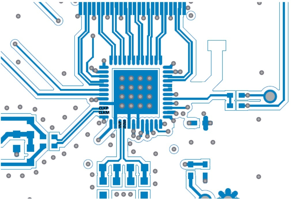
Layout Example

ADS4122 ADS4125 ADS4142 ADS4145 LAYOUTEX.png Figure 165. ADS412x and ADS414x EVM PCB Layout