ZHCS921A May 2012 – January 2016 ADS4128
PRODUCTION DATA.
- 1 特性
- 2 应用
- 3 说明
- 4 修订历史记录
- 5 Device Comparison Table
- 6 Pin Configuration and Functions
-
7 Specifications
- 7.1 Absolute Maximum Ratings
- 7.2 ESD Ratings
- 7.3 Recommended Operating Conditions
- 7.4 Thermal Information
- 7.5 Electrical Characteristics
- 7.6 Electrical Characteristics: General
- 7.7 Digital Characteristics
- 7.8 Timing Requirements: LVDS and CMOS Modes
- 7.9 Reset Timing Requirements
- 7.10 Typical Characteristics
- 7.11 Typical Characteristics: Contour
-
8 Detailed Description
- 8.1 Overview
- 8.2 Functional Block Diagram
- 8.3 Feature Description
- 8.4 Device Functional Modes
- 8.5 Programming
- 8.6 Register Maps
- 9 Application and Implementation
- 10Power Supply Recommendations
- 11Layout
- 12器件和文档支持
- 13机械、封装和可订购信息
9 Application and Implementation
NOTE
Information in the following applications sections is not part of the TI component specification, and TI does not warrant its accuracy or completeness. TI’s customers are responsible for determining suitability of components for their purposes. Customers should validate and test their design implementation to confirm system functionality.
9.1 Application Information
9.1.1 Analog Input
The analog input consists of a switched-capacitor-based, differential, sample-and-hold architecture. This differential topology results in very good ac performance even for high input frequencies at high sampling rates. The INP and INM pins must be externally biased around a common-mode voltage of 0.95 V, available on the VCM pin. For a full-scale differential input, each input INP and INM pin must swing symmetrically between (VCM + 0.5 V) and (VCM – 0.5 V), resulting in a 2-VPP differential input swing. The input sampling circuit has a high
3-dB bandwidth that extends up to 550 MHz (measured from the input pins to the sampled voltage). Figure 43 shows an equivalent circuit for the analog input.
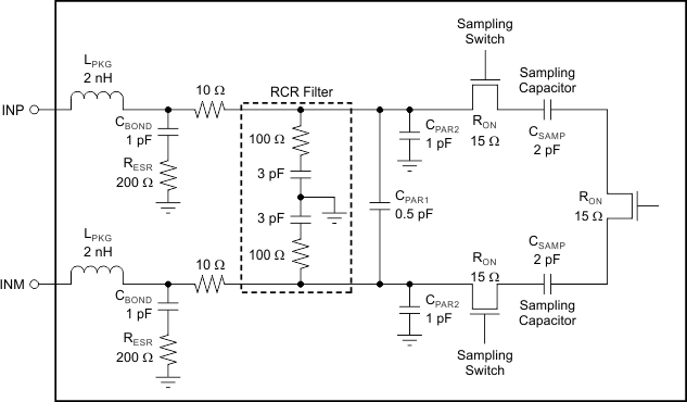 Figure 43. Analog Input Equivalent Circuit
9.1.2 Driving Circuit
Two example driving circuit configurations are shown in Figure 44 and Figure 45—one is optimized for low bandwidth and the other is optimized for high bandwidth to support higher input frequencies. In Figure 44, an external R-C-R filter with 3.3 pF is used to help absorb sampling glitches. The R-C-R filter limits the drive circuit bandwidth, making it suitable for low input frequencies (up to 250 MHz). Transformers such as ADT1-1WT or WBC1-1 can be used up to 250 MHz.
For higher input frequencies, the R-C-R filter can be dropped. Together with the lower series resistors (5 Ω to
10 Ω), this drive circuit provides higher bandwidth to support frequencies up to 500 MHz (as shown in Figure 45). A transmission line transformer (such as ADTL2-18) can be used.
Note that both drive circuits are terminated by 50 Ω near the ADC side. The termination is accomplished by a 25-Ω resistor from each input to the 0.95-V common-mode (VCM) from the device. This termination allows the analog inputs to be biased around the required common-mode voltage.
 Figure 44. Drive Circuit with Low Bandwidth (for Low Input Frequencies)
 Figure 45. Drive Circuit with High Bandwidth (for High Input Frequencies)
The transformer parasitic capacitance mismatch (between the windings) results in degraded even-order harmonic performance. Connecting two identical RF transformers back-to-back helps minimize this mismatch and good performance is obtained for high-frequency input signals. An additional termination resistor pair may be required between the two transformers; refer to Figure 44 and Figure 45. The termination center point is connected to ground to improve the balance between the P (positive) and M (negative) sides. The termination values between the transformers and on the secondary side must be chosen to obtain an effective 50 Ω (for a 50-Ω source impedance).
Figure 44 and Figure 45 use 1:1 transformers with a 50-Ω source. As explained in the Drive Circuit Requirements section, this architecture helps to present a low source impedance to absorb sampling glitches. With a 1:4 transformer, the source impedance is 200 Ω. The higher source impedance is unable to absorb the sampling glitches effectively and can lead to degradation in performance (compared to using 1:1 transformers).
In almost all cases, either a band-pass or low-pass filter is needed to get the desired dynamic performance, as shown in Figure 46. Such a filter presents low source impedance at the high frequencies corresponding to the sampling glitch and helps avoid performance loss with the high source impedance.
 Figure 46. Drive Circuit with 1:4 Transformer
9.1.2.1 Drive Circuit Requirements
For optimum performance, the analog inputs must be driven differentially. This technique improves the common-mode noise immunity and even-order harmonic rejection. A 5-Ω to 15-Ω resistor in series with each input pin is recommended to damp out ringing caused by package parasitics. It is also necessary to present low impedance (less than 50 Ω) for the common-mode switching currents. This impedance can be achieved by using two resistors from each input terminated to the common-mode voltage (VCM).
Note that the device includes an internal R-C filter from each input to ground. The purpose of this filter is to absorb the glitches created when the sampling capacitors open and close. The R-C filter cutoff frequency involves a trade-off. A lower cutoff frequency (larger C) absorbs glitches better, but also reduces the input bandwidth and maximum input frequency that can be supported. On the other hand, with no internal R-C filter, high input frequency can be supported but now the sampling glitches must be supplied by the external driving circuit. The inductance of the package bond wires limits the ability of the external driving circuit to support the sampling glitches.
In the ADS4128, the R-C component values have been optimized while supporting high input bandwidth
(550 MHz). However, in applications where very high input frequency support is not required, glitch filtering can be further improved with an external R-C-R filter; see Figure 44 and Figure 45).
In addition, the drive circuit may have to be designed to provide a low insertion loss over the desired frequency range and matched source impedance. While designing the drive circuit, the ADC impedance must be considered. Figure 47 and Figure 48 show the impedance (ZIN = RIN || CIN) looking into the ADC input pins.
 Figure 47. ADC Analog Input Resistance (RIN) Across Frequency
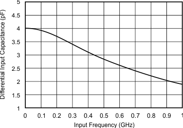 Figure 48. ADC Analog Input Capacitance (CIN) Across Frequency
9.1.3 Analog Input
9.1.3.1 Input Common-Mode
To ensure a low-noise, common-mode reference, the VCM pin is filtered with a 0.1-µF low-inductance capacitor connected to ground. The VCM pin is designed to directly drive the ADC inputs. Each ADC input pin sinks a common-mode current of approximately 0.6 µA per MSPS of clock frequency.
9.1.4 Clock Input
The ADS4128 clock inputs can be driven differentially (sine, LVPECL, or LVDS) or single-ended (LVCMOS), with little or no difference in performance between them. The common-mode voltage of the clock inputs is set to VCM using internal 5-kΩ resistors. This setting allows the use of transformer-coupled drive circuits for sine-wave clock or ac-coupling for LVPECL and LVDS clock sources. Figure 49 shows an equivalent circuit for the input clock.

A single-ended CMOS clock can be ac-coupled to the CLKP input, with CLKM connected to ground with a 0.1-μF capacitor, as shown in Figure 50. For best performance, the clock inputs must be driven differentially, reducing susceptibility to common-mode noise. For high input frequency sampling, it is recommended to use a clock source with very low jitter. Band-pass filtering of the clock source can help reduce the effects of jitter. There is no change in performance with a non-50% duty cycle clock input. Figure 51 shows a differential circuit.
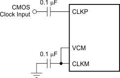 Figure 50. Single-Ended Clock Driving Circuit
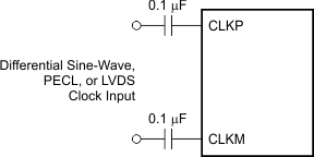 Figure 51. Differential Clock Driving Circuit
9.2 Typical Application
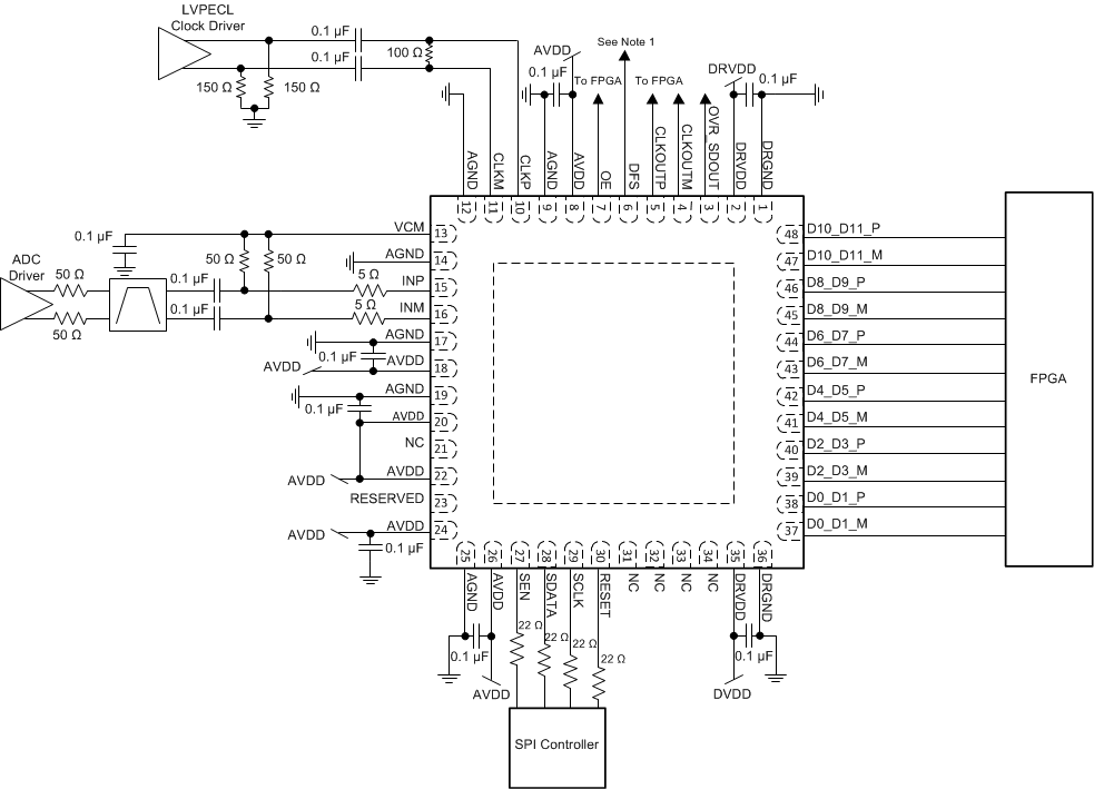
An example schematic for a typical application of the ADS4128 is shown in Figure 52.
9.2.1 Design Requirements
Example design requirements are listed in Table 13 for the ADC portion of the signal chain. These do not necessary reflect the requirements of an actual system, but rather demonstrate why the ADS4128 may be chosen for a system based on a set of requirements.
Table 13. Example Design Requirements for ADS4128
| DESIGN PARAMETER | EXAMPLE DESIGN REQUIREMENT | ADS4128 CAPABILITY |
|---|---|---|
| Sampling rate | ≥184.32 Msps | Max sampling rate: 200 Msps |
| Input frequency | >190 MHz to accommodate full 2nd nyquist zone | Large signal –3 dB bandwith: 400 MHz operation |
| SNR | >65dBFS at –1 dFBS 170 MHz | 69 dBFS at –1 dBFS, 170 MHz |
| SFDR | >80 dBc at –1 dFBS 170 MHz | 85 dBc at –1 dBFS, 170 MHz |
| Input full scale voltage | 2 Vpp | 2 Vpp |
| Overload recovery time | < 3 clock cycles | 1 clock cycle |
| Input full scale voltage | Parallel LVDS | Parallel LVDS |
| Overload recovery time | < 250 mW per channel | 230 mW per channel |
9.2.2 Detailed Design Procedure
9.2.2.1 Analog Input
The analog input of the ADS4128 is typically driven by a fully differential amplifier. The amplifier must have sufficient bandwidth for the frequencies of interest. The noise and distortion performance of the amplifier affects the combined performance of the ADC and amplifier. The amplifier is often AC coupled to the ADC to allow both the amplifier and ADC to operate at the optimal common-mode voltages. The user can DC couple the amplifier to the ADC if required. An alternate approach is to drive the ADC using transformers. DC coupling cannot be used with the transformer approach.
9.2.2.2 Clock Driver
The ADS4128 should be driven by a high performance clock driver such as a clock jitter cleaner. The clock must have low noise to maintain optimal performance. LVPECL is the most common clocking interface, but LVDS and LVCMOS can also be used. Do not drive the clock input from an FPGA unless the noise degradation can be tolerated, such as for input signals near DC where the clock noise impact is minimal.
9.2.2.3 Digital Interface
The ADS4128 supports both LVDS and CMOS interfaces. The LVDS interface should be used for best performance when operating at maximum sampling rate. The LVDS outputs can be connected directly to the FPGA without any additional components. When using CMOS outputs, resistors must be placed in series with the outputs to reduce the output current spikes and limit the performance degradation. The resistors must be large enough to limit current spikes, but not so large as to significantly distort the digital output waveform. An external CMOS buffer must be used when driving distances greater than a few inches, to reduce ground bounce within the ADC.
9.2.3 Application Curve
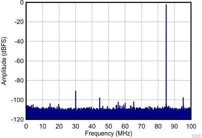
Figure 53 shows the result of a 115-MHz signal sampled at 200 MHz captured by the ADS4128
| SNR = 70.13 dBFs | SFDR= 83.75 dBFs | |
| THD= 79.72 dBs | SINAD= 69.90 dBFs |